



Education Journalist | Study Abroad Lead
Digital electronics is a branch of electronics that deals with the study of digital signals, circuits, and the devices used to produce them. Logic gates, digital cameras, digital televisions, smartphones, computer, and their memory components, etc. are examples of digital devices. In digital electronics, a gate is a logic circuit that has one or more inputs but produces an only single output. The output signal is obtained for only certain combinations of input signals depending upon the circuits. Logic gates work on the Boolean function and produce an output concerning input.
| Table of Content |
Key Terms: Logic Gates, OR gate, AND gate, NOT gate, NAND gate, NOR gate
Logic Gates
[Click Here for Sample Questions]
In digital electronics, a gate is a logic circuit that has one or more inputs but produces only single output. The output signal is obtained for only certain combinations of input signals depending upon the circuits. Logic gates work on the Boolean function and produce an output concerning input.
Logic gates are the basic building components of any digital system. It has one or more inputs but produces a single output.
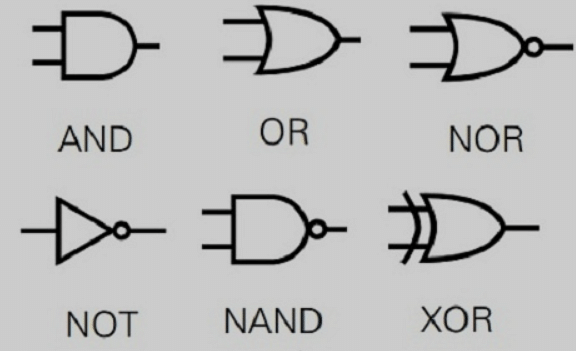
Logic Gate Symbols
Here we shall consider five logic gates namely OR, AND, NOT, NAND, NOR with their Boolean function and truth table.
The function of logic gates can be analyzed using semiconductor devices.
Also Read:
OR Gate
[Click Here for Sample Questions]
The OR gate has one or more inputs but produces only single output. If any one of the given inputs is high then the output will also high. Thus if there are N inputs A, B, C, ..., N, then output Y equals A or B or C...or N.
If there are two inputs A and B then output of OR gate will be given by following mathematical operation:
Y = A + B
Here + sign represents OR logical operation

The truth table of OR gate
| Input | Output | |
|---|---|---|
| A | B | Y = A + B |
| 0 | 0 | 0 |
| 0 | 1 | 1 |
| 1 | 0 | 1 |
| 1 | 1 | 1 |
Application of OR gate
The function of the OR gate can be observed using a circuit with two parallel switches. The circuit diagram of OR gate is shown below :

The Function of the OR gate
The bulb will glow if only one switch is closed and at least one switch will be open. It can be verified using a truth table. If both the switches are open then the bulb will not glow.
AND Gate
[Click Here for Sample Questions]
The AND gate has also two or more inputs but it produces only single output. The output will be obtained 1 only when both the given inputs are 1. This if there are N inputs A, B, C, ....., N, the output Y equals to A and B and C and..... and N. The Boolean equation for AND gate is shown below :
Y = A. B or Y = A × B
Here (.) or × sign represents AND logical operation

AND gate symbol
The truth table of AND gate
| Input | Output | |
|---|---|---|
| A | B | Y = A.B |
| 0 | 0 | 0 |
| 0 | 1 | 0 |
| 1 | 0 | 0 |
| 1 | 1 | 1 |
Application of AND gate
The function of AND gate can be analyzed by connecting two switches in series. The circuit diagram of AND gate is shown below :

In this circuit, the bulb will glow only when both switches are closed and if any input will be 0 then the light will not glow or off.
NOT Gate
[Click Here for Sample Questions]
The NOT gate is a fundamental gate that has one input and one output. It changes the polarity of the input signal. Thus for input A, the output Y equals NOTA, i.e., the output is not the same as the input. The Boolean expression for NOT gate is shown below :
Y = NOT A or A
Here bar sign indicates NOT operation.

NOT gate symbol
The truth table of NOT gate
| Input | Output |
|---|---|
| A | Y = NOT A or A |
| 0 | 1 |
| 1 | 0 |
Application of NOT gate
The function of the NOT gate can be observed by connecting a transistor in common emitter mode in the circuit. When no input is applied at the base (A=0) the transistor is cut off and no collector current flows, so the output is due to collector supply voltage is 1.

When the input is applied at the base (i.e. A =1) transistor operates and the collector current flows in load resistance R in opposite phase, so the voltage across R annuls the collector supply voltage and no output is obtained at the inverter gate.
NAND Gate
[Click Here for Sample Questions]
NAND gate is a combination of two logic gates namely NOT and AND gate. If both inputs A and B are 1 then the output will not be 1. NAND gates are also called universal logic gates since using universal gates the basic gates can be easily realized. The Boolean expression for NAND gate is shown below :
Y = A.B

NAND gate symbol
The Truth table of NAND gate
| Input | Output | |
|---|---|---|
| A | B | Y = A.B |
| 0 | 0 | 1 |
| 0 | 1 | 1 |
| 1 | 0 | 1 |
| 1 | 1 | 0 |
Application of NAND gate
The function of the NAND gate can be observed by combining both NOT and AND logic gates. The electric circuit for the NAND gate is shown below :

The logic operation of the NAND gate is inverse of the basic AND gate.
NOR Gate
[Click Here for Sample Questions]
The NOR gate is a combination of two basic logic gates namely NOT and OR gates. It has two or more inputs but the output is single. Its output will be 1 only when both inputs A and B are 0.
NOR gates are also universal gates because using these the basic gates can be easily obtained. The Boolean expression for NOR gate is shown below:
Y = A+B

NOR gate symbol
The Truth table of NOR gate
| Input | Output | |
|---|---|---|
| A | B | Y = A+B |
| 0 | 0 | 1 |
| 0 | 1 | 0 |
| 1 | 0 | 0 |
| 1 | 1 | 0 |
Circuit diagram of NOR gate
The circuit diagram of NOR gate to observe its function is shown below :

Circuit Diagram Of NOR Gate
Also Read:
Sample Questions
Ques. What are logic gates? (1 mark)
Ans - The digital electronic circuits used to perform the logic operation as per the given inputs produce an output.
Ques. Name the different types of logic gates? (1 mark)
Ans - Commonly three fundamental logic gates viz. AND, OR, and NOT. With using these basic gates many logic gates can be obtained namely NAND, NOR, XOR, XNOR, etc.
Ques. Which of the following logic gate is also known as invertor?
a) AND gate. b) OR gate
c) NOT gate. d) NOR (1 mark)
Ans : c) NOT gate is known as an invertor because it inverts the polarity of the input signal.
Ques. What are universal gates? Name any two universal gates? (1 mark)
Ans - The gates are generated by combining two or more basic gates to perform a certain logical operation called universal gates. NAND gate and NOR gate are the universal gates.
Ques. If the input is 1 in NOT gate then the resultant output will be? (1 mark)
Ans - The NOT gate works as an invertor, if input 1 is applied to it then the output will be 0, or for input 0 output will be 1.
Ques. From which logic gates we can obtain basic logic gates? (1 mark)
Ans - The basic logic gates can be obtained from universal gates. With using NAND and NOR logic gates the basic gates like OR, AND, NOT gates can be obtained by different configurations.
Ques. Give the Boolean expression for AND gate? (1 mark)
Ans - The Boolean expression for AND gate is Y = A.B. Here A and B are given inputs and Y is an output equal to A.B.
Ques. Give the Boolean expression for OR logic gate? (1 mark)
Ans - The Boolean expression for OR logic gate is Y = A+B. For inputs A and B, the output will be A or B i.e. A+B.
For Latest Updates on Upcoming Board Exams, Click Here: https://t.me/class_10_12_board_updates
Check-Out:



Comments