



Education Journalist | Study Abroad Lead
Zener Diode is a semiconductor device which conducts current in both forward bias and reverse bias. A zener diode allows electricity to travel from anode to cathode. It enables the current to flow in the reverse direction on reaching the Zener voltage. When a particular voltage is achieved, the heavily doped PN junction of the Zener diode conducts the current in the reverse direction. Zener diodes are the most widely applicable semiconductor diodes.
Related Links
- Appearing for JEE Main, Download JEE Mains PYQ for all sabjects
- Appearing for NEET, Download NEET PYQ for all subjects
| Table of Content |
Key Terms: Zener Voltage, Semiconductor Diode, Zener Effect, Avalanche Breakdown, Zener Breakdown, Forward Characteristics, Reverse Characteristics
What is Zener Diode?
[Click Here for Sample Questions]
Zener Diode or breakdown diode is a heavily doped semiconductor device. Zener diode also works in the reverse direction. The current flows in the reverse direction when the heavily doped PN junction breaks down. This happens when the voltage across the terminals of a Zener diode is reversed. Owing to this, the potential reaches the Zener Voltage (knee voltage). This effect is known as the Zener Effect.
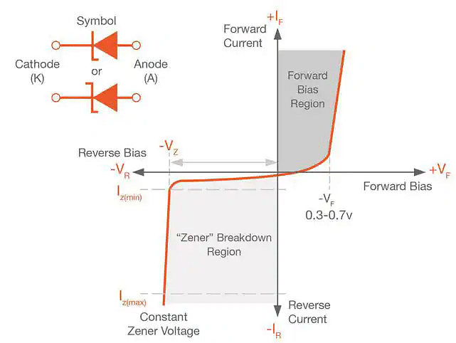
Zener Diode Diagram
The video below explains this:
Zener Diode as a Voltage Regulator Detailed Video Explanation:
Also check:
How does a Zener Diode work in Reverse Bias?
[Click Here for Previous Year Questions]
- Zener Diode works similarly to a normal diode in the forward-biased mode.
- However, in the reverse biased mode, a small leakage current is passed through the diode.
- There’s an increase in the reverse voltage to the predetermined breakdown voltage (Vz).
- The breakdown leads to the flow of current through the diode.
- The current rises to a maximum, which relies on the series resistor.
- After this, it stabilizes and remains consistent throughout a wide range of applied voltage.
There are two types of breakdowns for a Zener Diode:
Avalanche Breakdown in Zener Diode
- Avalanche breakdown can take place in case of high reverse voltage both in normal diode and Zener Diode.
- A high value of the reverse voltage on the PN junction provides energy to the free electrons and accelerates them at high velocities.

Avalanche Breakdown
- The free electrons moving at high velocity collide with other atoms and knock off more electrons.
- Due to this constant collision, several free electrons are generated.
- This is associated with the constant increase in electric current in the diode.
- The sudden increase in electric current can permanently destroy the normal diode.
- However, a Zener diode is designed to work under avalanche breakdown.
- Avalanche breakdown usually occurs in Zener diodes with Zener voltage higher than 6V.
Zener Breakdown in Zener Diode
- The applied reverse bias voltage reaches closer to the Zener voltage.
- When this happens, the electric field in the depletion area gets stronger.
- With this, the electrons get pulled away from their valence band.
- Valence electrons that gain enough energy from the depletion region's strong electric field pull away from the parent atom.
- An increase in voltage leads to a rapid increase in electric current at the Zener breakdown region.

Zener Breakdown
Avalanche Breakdown vs Zener Breakdown
The key differences between Avalanche Breakdown and Zener Breakdown are tabulated below:
| Parameters | Zener Breakdown | Avalanche Breakdown |
|---|---|---|
| Definition | It occurs in the Zener diodes having Vz between 5 to 8 volts or less than 5V. | Avalanche breakdown occurs in the p-n junction when the Vz is greater than 8 volts. |
| Depletion region | The depletion region is thin. | The depletion region is thick. |
| Electric connection | The connection is not destroyed. | Connection is destroyed. |
| Electric field | The electric field is strong. | The electric field is weak. |
| Temperature coefficient | Negative | Positive |
| Voltage proportion to the temperature | Inversely proportional | Directly proportional |
| Structure | PN junction diode | Highly developed p and n region |
Zener Diode Circuit Symbol
[Click Here for Sample Questions]
There are many ways in which a Zener diode is packaged. Some are used for high levels of power dissipation and the others are contained with surface mount formats. The most common type of Zener diode is contained within a small glass encapsulation. It has a band around one end marking the cathode side of the diode.
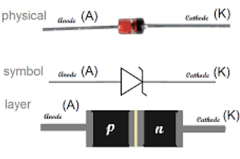
The above diagram shows that the band around the package is corresponding to the line on the diode circuit symbol. This can help in associating one end with the other.
Zener Diode Circuit Symbol places two tags at the end of the bar. One tag goes in the upward direction and the other one goes in the lower direction. This helps in distinguishing Zener diodes from other diodes within the circuit.
V-I Characteristics of Zener Diode
[Click Here for Previous Year Questions]
The VI Characteristics of Zener diode have been divided into two parts:

Forward Characteristics of Zener Diode
The forward properties of Zener diode are represented in the graph's first quadrant. The graph shows that the forward characteristics are nearly identical to those of any other P-N junction diode.
Reverse Characteristics of Zener Diode
When a reverse voltage is passed into a Zener voltage, a tiny reverse saturation current Io flows across the diode at first. This current is caused by minority carriers that are produced thermally.
When the reverse voltage is increased to a particular level, the reverse current increases dramatically and quickly. This indicates that a breakdown has happened. This voltage breakdown voltage, also known as Zener voltage, is indicated by Vz.
Zener Diode Specifications
[Click Here for Sample Questions]
Specifications of Zener diode vary in different aspects such as voltage, power dissipation, maximum reverse current, etc. Some of its specifications are as follows.
- Voltage (Vz): The Zener voltage or reverse breakdown voltage ranges between – 2.4V to 200V. Although the Zener voltage can go up to 1kV, the maximum voltage for a Surface Mounted Device (SMD) is about 47V.
- Current (Iz)(Max): It is the maximum current that occurs at the rated Zener Voltage (Vz: 200\(\mu\)A to 200A)
- Current (Iz)(Min): It is the minimum current that is required for the Zener diode to breakdown (Iz: 5mA to 10mA)
- Power Rating: Power rating is the maximum energy dissipated by the Zener diode and it is given by the product of voltage of the diode and the current flowing through it. Common power rating values are 400mW, 500mW, 1W, 5W.
- Voltage Tolerance: It has a typical value of ±5%
- Temperature Stability: Zener Diodes having voltage around 5V have the best temperature stability.
- Zener Resistance (Rz): It is the resistance offered by the Zener diode which is visible in its IV characteristics.
Zener Diode Applications
[Click Here for Previous Year Questions]
Some of the applications of zener diode are as follows:
Zener Diode as a Voltage Regulator
- Zener diode is used as a Shunt voltage regulator to regulate the voltage across small loads. Zener diodes have a consistent breakdown voltage over a large current range.
- Zener diode is connected in parallel to the load to reverse bias it, and once it surpasses the knee voltage, the voltage across the load becomes constant.
Zener Diode in Over-voltage Protection
- Zener diodes are useful for protecting power supply lines and power supply control lines, as well as internal circuits and integrated circuits (ICs) against overvoltages caused by hot plugs.
- Static electricity (ESD) and other overvoltage pulses can cause damage to the power supply line, which must be protected. Zener diodes make it simpler and safer to secure circuits and ICs.

| Uses of Zener Diode
|
Read More:
Things to Remember
- Zener diode is a semiconductor device that allows current to flow in a forward or reverse direction.
- Zener diode is often used as a shunt voltage regulator. To reverse bias the load, a Zener diode is connected parallel to it, and after the Zener diode surpasses knee voltage, the voltage across the load becomes constant.
- The flow of current is the main difference between a Zener diode and a regular diode. A normal diode can only flow in one direction, but a Zener diode can flow in both directions.
- The maximum current that can pass through a Zener diode is called Iz-max. There is usually a minimum current required for its operation. For a standard 400 mW led, this can range from 5 to 10 mA.
Previous Year Questions
- The ratio of forward to reverse bias resistance is? [VITEEE 2018]
- A n−p−n transistor conducts when..? [NEET 2003]
- A n−p−n transistor is connected to common emitter configuration in a given amplifier. A load resistance of…? [NEET 2016]
- A p−n photodiode is made of a material with a band gap of 2eV. The minimum frequency…? [NEET 2008]
- A piece of copper and other of germanium are cooled from the room temperature to 80 K, then…? [NEET 1992]
- A Zener diode, having breakdown voltage equal to 15V … [NEET 2011]
- Zener diode is used for … [NEET 2005]
- In a common emitter transistor amplifier the audio signal voltage across the collector is…? [NEET 2017]
- p-n junction is said to be forward biased, when..? [NEET 1998]
- At absolute zero, Si acts as..? [NEET 1998]
- A common emitter amplifier has a voltage gain of 50, an input impedance of 100Ω and an…? [NEET 2010]
- A Zener diode is connected to a battery and a load … [JEE Mains 2014]
- In the given circuit, the current through zener diode … [JEE Mains 2018]
- Voltage rating of a parallel plate capacitor is 500V … [JEE Mains 2019]
- A semiconducting device is connected in a series circuit … [NEET 1998]
- A junction diode has a resistance of … [WBJEE 2009]
- The barrier potential of a p−np−n junction depends … [NEET 2014]
Sample Questions
Ques. Why does Zener breakdown occur? (2 Marks)
Ans. Zener breakdown occurs either due to the Zener breakdown effect which occurs when the voltage is below 5.5 V or due to the impact of ionization which occurs above 5.5 V. Both of these mechanisms occur in the same circuit.
However, they have different temperature coefficients. The impact effect has a positive temperature coefficient, while the Zener effect has a negative temperature coefficient. The two temperature effects occur at an equal voltage of around 5.5V and cancel out each other, thus making the Zener diode operate at 5.5V.
Ques. What is a Voltage Regulator? (2 Marks)
Ans. A voltage regulator is a device that regulates the voltage level. It essentially steps down the input voltage to the desired level and keeps it at that same level during the supply. This ensures that even when a load is applied the voltage doesn’t drop. The voltage regulator is used for two main reasons, and they are:
- To vary or regulate the output voltage
- To keep the output voltage constant at the desired value despite variations in the supply voltage.
Voltage regulators are used in computers, power generators, alternators to control the output of the plant.
Ques. In the circuit diagram of the Zener diode as shown in the figure, when the value of V0 is 8 volt, the current through Zener diode s i1, and when V0 is 16 volt, the corresponding current is i2. Find the value of (i2−i1). (Zener breakdown voltage = V2 =6V). (3 Marks)

Ans. For V0 = 8 Volt
i0 = 8-6/1000 = 2 mA; i2 = 6/4000 = 1.5 mA
∴ i1 = (2−1.5) = 0.5 mA
for V0 =16 Volt; i’0 = 10/1000 = 10mA’i’2 = 1.5 mA
∴ i’1 = 10−1.5 =8.5 mA
⇒i’1-i1 = 8 mA

Ques. Mention the key differences between Zener Breakdown and Avalanche Breakdown. (4 Marks)
Ans.
| Parameters | Zener Breakdown | Avalanche Breakdown |
|---|---|---|
| Graph curve | It has a sharp curve | It doesn’t have a sharp curve |
| Mechanism | It occurs because of the high electric field | It occurs because of the collision of free electrons |
| Tunneling effect | The tunneling effect takes place | The tunneling effect is absent |
| Doping concentration | The doping concentration is high at the junction | The doping at the junction is minimum |
| Electrons and holes | The production of electrons takes place. | The production of a pair of electrons and holes takes place. |
| Voltage | The breakdown doesn’t affect the voltage | After the breakdown, the voltage tends to vary |
| Effect on junction | The junction gets back to the normal position after the voltage is removed | The junction is destroyed permanently |
Ques. Give some Zener diode specifications. (5 Marks)
Ans. Zener diodes vary in specifications like the nominal working voltage, maximum reverse current, power dissipation, and packaging. Some of the commonly used specifications are:
Voltage Vz: Zener voltage refers is the reverse breakdown voltage, which ranges from 2.4 V to 200 V; and can go up to 1 kV in maximum case the surface-mounted device (SMD) is about 47 V).
Current lz (min.): The minimum current required to break down the diode is 5 mA- 10 mA.
Current lz (max.): The maximum current of the rated Zener voltage (Vz) is 200 uA - 200 A).
Voltage tolerance: It is normally ±5%.
Power rating: The maximum power which can be dissipated by the Zener diode is calculated by the product of the current flowing through the diode and the voltage across the diode. Normal values of power rating are 400 mW, 500 mW, 1 W, and 5 W. for surface mounting, 200 mW, 350 mW, 500 mW, and 1 W are the normal values.
Temperature stability: Diodes operating around 5 V have the best stability.
Package: Lead device and the surface mounts either within integrated circuits or as discrete devices.
Zener resistance (Rz): The diode exhibits some resistance which is shown from the IV characteristics.
Ques. For the circuit shown in Fig.1 (i), find:
(i) the output voltage
(ii) the voltage drop across series resistance
(iii) the current through zener diode. (5 Marks)
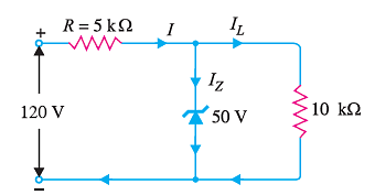
Fig.1 (i)
Ans. Upon removing the zener diode in Fig. 1, voltage V across the open-circuit is shown as:
\(V = \frac{R_LE_i}{R+R_L} = \frac{10 \times 120}{5 + 10} = 80 V\)
Voltage across zener diode is higher than VZ (= 50 V), zener is in the “on” state. It can thus be represented by a battery of 50 V as shown in Fig. 1 (ii).

With reference to Fig. 1 (ii),
Output Voltage = VZ = 50 V
(ii) Voltage Drop across R= Input Voltage – VZ = 120-50 = 70 V
(iii) Load Current, IL = VZ/RL = 50 V/10 k\(\Omega\) = 5 mA
Current through R, I = 70 V/5 k\(\Omega\) = 14 mA
Applying Kirchhoff’s first law, I = IL + IZ
Thus, Zener Current, IZ = I – IL = 14 – 5 = 9 mA
Ques. How does behavior of zener diode differ substantially from that of a normal (rectifying) diode? (1 Mark)
Ans. Zener diodes break down at substantially lower reverse voltages than rectifying diodes, and their breakdown voltages are predictable.
Ques. Qualitatively determine what will happen to the series resistor current and the zener diode current in this voltage regulator circuit if the load current suddenly decreases. Assume that the zener diode’s behavior is ideal; i.e. its voltage drop holds absolutely constant throughout its operating range.
IRseries = (increase, decrease, or unchanged?)
Izener = (increase, decrease, or unchanged?) (1 Mark)
Ans. If the load current decreases, Izener will increase and IRseries will remain unchanged.
Ques. The electric field required for the field ionization is of what order?
a) 104 V/m
b) 105 V/m
c) 106 V/m
d) 107 V/m (2 Marks)
Ans. In a Zener diode, a very high electric field is produced for even a very small voltage. The electric field required for field ionization is of the order 106 V/m.
Ques. How does a Zener diode different from a normal diode? (1 mark)
Ans. The main difference between a Zener diode and a normal diode lies in the fact that in the passage of current. A normal diode allows current to flow only in one direction while a Zener diode allows current to flow in both directions.
Ques. On which factor does the reverse breakdown voltage depend? (2 marks)
Ans. The reverse breakdown depends upon the level of doping of the re-type and p-type sections of the diode. General-purpose diodes have each section lightly doped. They have a high value of reverse breakdown voltage. Zener diodes have each section heavily doped. They have a low value of reverse breakdown voltage.
For Latest Updates on Upcoming Board Exams, Click Here: https://t.me/class_10_12_board_updates
Do Check Out:



Comments