



Education Journalist | Study Abroad Lead
Semiconductors are materials having conductivity properties lying between good conductors and insulators of electricity. Some notable examples of semiconductors are germanium and arsenic. The two types of semiconductors are intrinsic or pure semiconductors and extrinsic or impure semiconductors. Charge carriers responsible for current flow in semiconductors are holes and electrons. Both are equal in magnitude but opposite in polarity. Holes are positively charged carriers while electrons are negatively charged carriers.
| Table of Content |
Key Terms: Intrinsic Semiconductors, Extrinsic, Semiconductors, Mobility, Rectifier Efficiency, Amplification Factor, Transistors, Electrons, Holes
Intrinsic and Extrinsic Semiconductors
[Click Here for Sample Questions]
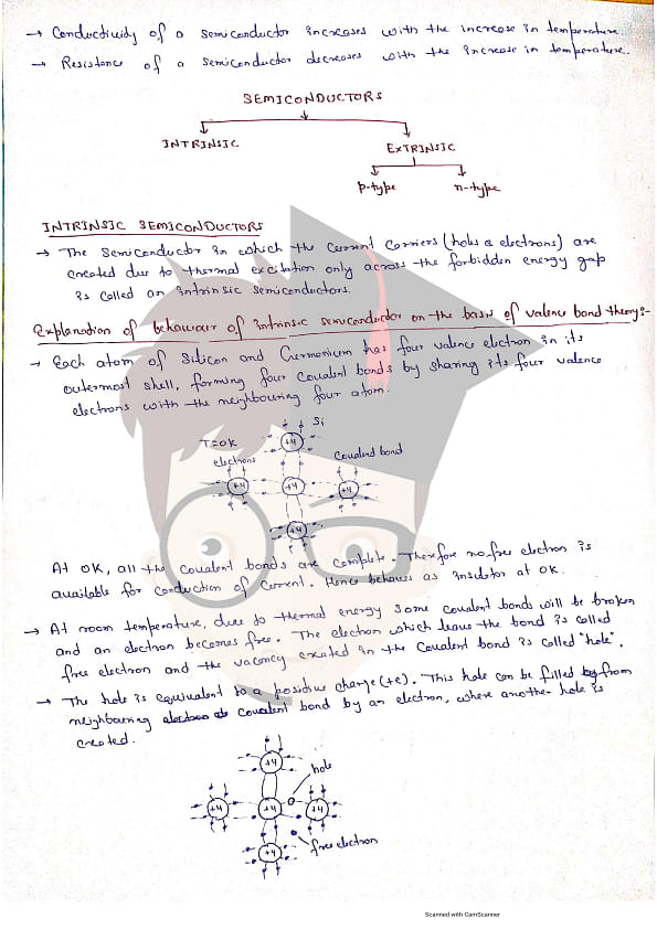
- Intrinsic semiconductors are pure semiconductors having charge carriers (electrons and holes) produced due to thermal excitation that represent the intrinsic property of the material. No impurity of atoms is added to increase the conductivity during intrinsic conduction that occurs by electron-hole pairs.
- In intrinsic semiconductors, the number of electrons in conduction band is equal to the number of holes in the valence band,nh. Therefore, the intrinsic charge carrier concentration, ni=ne=nh.
- Extrinsic semiconductors are impure semiconductors that are made by doping pure semiconductors with impure atoms to increase conductivity. The number of electrons and holes can be changed by this method of doping.
- There are two types of extrinsic semiconductors, n-type and p-type semiconductors.
- In n-type semiconductors, electrons are the majority carriers while holes are the minority charge carriers, that is, nenh.
- In p-type semiconductors, holes are the majority charge carriers while electrons are the minority charge carriers, that is, nhne.
The video below explains this:
Semiconductors and Insulators Detailed Video Explanation:
Semiconductor Electronics Class 12 Important Notes PDF
Semiconductor Electronics Class 12 Important Notes




Also Read:
| Related Articles | ||
|---|---|---|
| Transistor | Difference between LCD and LED | Rectifier |
| Zener Diode | Bridge Rectifier | Application of Junction Diode |
Mobility
[Click Here for Sample Questions]
- The mobility of charge carriers can be defined as the magnitude of drift velocity per unit electric field applied.
- The term mobility is represented by the symbol, . If the drift velocity and electric field are represented as Vd and E respectively, then the mobility is given by, =VdE
- The SI unit of mobility is m2V-1s-1.
- The mobility of electrons( e) is greater than the mobility of holes (h), that is, e>h
Transistors
[Click Here for Sample Questions]
- Transistors are three-section semiconductors, used as amplifiers and oscillators that help in the conduction and insulation of electric current or voltage. They are of two types, bipolar junction transistor and field-effect transistor. The three sections of the transistors are emitter, collector, and base.
- The emitter current (Ie) is always slightly greater than the collector current, and is given as the sum of collector current (Ic) and base current (Ib), that is, Ie=Ic+Ib
- Low current gains of a transistor are defined into two types, common base current amplification factor and common emitter current amplification factor.
- Common base current amplification factor or ac current gain () is defined as the ratio of small change in the collector current to the small change in the emitter current when the collector-base voltage is kept constant, that is, =IEIC, where VCB=constant.
- Common emitter current amplification factor or ac current gain () is defined as the ratio of small change in the collector current to the small change in the base current when the collector-emitter voltage is kept constant, that is, =IEIB, where VCE=constant.
- The relation between the current gains, and are given by, =1+ and =1-
Power Gain
[Click Here for Sample Questions]
- The ac power gain is defined as the ratio of change in output power to the change in input power.
- The formula for ac power gain is given by, Power gain= (Ic)Rout(Ib)Rin, where RoutRin is the resistance gain.
Logic Gates
[Click Here for Sample Questions]
- Logic gates are Boolean function based digital devices used to carry out logical operations.
- If A and B are the given inputs, then the output, C is given as, C=A+B.
- There are different types of logic gates namely, AND, OR, NAND, NOR, and NOT gates, and the output in these can be calculated as follows:
| Logic Gate | Output, C |
| AND gate | C=A |
| OR gate | C=AB |
| NAND gate | C=AB |
| NOR gate | C=A+B |
| NOT gate | C=A or C=B (either A or B is present) |
Things to Remember
- The electron density in the conduction band is equal to the hole density in the valence band for the case of intrinsic semiconductors.
- Extrinsic semiconductors are made by the process of doping through which the impurities are added to a pure semiconductor and hence the charge carrier can be changed.
- The mobility of charge carriers can be defined as the magnitude of drift velocity per unit electric field applied, that is, =VdE
- With the exponential increase in temperature, the electrical conductivity of intrinsic semiconductor increases. The formula for electrical conductivity is given by, =0exp(-Eg2kBT)
- The relation between the current gains, and are given by, =1+ and =1-
- The formula for ac power gain is given by, Power gain= (Ic)Rout(Ib)Rin, where RoutRin is the resistance gain.
- The emitter current (Ie) in a transistor is the sum of collector current (Ic) and base current (Ib), that is, Ie=Ic+Ib
Also Read:
Sample Questions
Ques. The semiconductor, GaAs, is commonly used in solar cells. Give reasons. (1 Mark)
Ans. GaAs is commonly used in solar cells because they have high conductivity and high optical absorption. Hence, GaAs is suitable in solar cells.
Ques. A transistor has a current gain of 30 and collector resistance of 6k. If the input resistance is 1k, calculate and find the voltage gain of the transistor. (2 Marks)
Ans. Input resistance,Rin=1k
Output resistance,Rout=6k
So, the resistance gain, Rgain=RoutRin
Rgain=61
Rgain=6
We know, that, voltage gain=Rgaincurrent gain
voltage gain=630
Hence, voltage gain=180
Ques. If the voltage gain is 120 and the current gain is 30, then find the resistance gain of the transistor. (2 Marks)
Ans. The voltage gain = 120 and the current gain = 30
We know that, voltage gain=Rgaincurrent gain
So, resistance gain,Rgain=voltage gaincurrent gain
resistance gain,Rgain=12030
resistance gain,Rgain=4 k
Ques. Find the ratio of the number of conduction electrons and the number of holes in an intrinsic semiconductor. (2 Marks)
Ans. We know that, in an intrinsic semiconductor, the number of conduction electrons present is equal to the number of holes, that is,
ne=nh
So, the ratio of the number of conduction electrons and the number of holes in an intrinsic semiconductor will be equal to one, that is,
nenh=1
Ques. What is mobility? Write its general formula. (1 Mark)
Ans. Mobility is defined as the drift velocity applied per unit electric field.
If the drift velocity and electric field are represented as Vd and E respectively, then the mobility is given by the formula, =VdE
Ques. How is reverse biasing different from forward biasing in a p-n junction diode? [Delhi 2001] (3 Marks)
Ans. Differences between forward bias and reverse bias are listed below:
| Forward Bias | Reverse Bias |
|---|---|
| The positive and negative terminals of the battery are connected to the p-type and n-type semiconductor of the device respectively. | The positive and negative terminals of the battery are connected to the n-type and p-type semiconductor of the device respectively. |
| Larger forward current | Smaller forward current |
| Thinner depletion layer | Thicker depletion layer |
| Lower resistance | Higher resistance |
| Allows current flow | Prevents current flow |
Ques. What is the criterion for charge carriers in intrinsic semiconductors? (1 mark)
Ans. For intrinsic semiconductors, the number of electrons in conduction band, ne is equal to the number of holes in the valence band,nh. Therefore, the intrinsic charge carrier concentration, ni=ne=nh.
Ques. Why is the conductivity of a semiconductor increasing with increase in temperature? (1 mark)
Ans. There is a decrease in relaxation time when the number density of charge carriers carrying current increases. This increase in number density of current carriers is much greater than the decrease in relaxation time. Hence,the conductivity of a semiconductor increases with increase in temperature.
Ques. The AC current gain of a transistor is 120 and its base current changes by 100A. Then, find the change in the collector current of the transistor. (2 mark)
Ans. We have, the AC current gain of a transistor,=120
Also, given that the base current changes by 100A
IB=100A
We know that, =IEIB, where VCE=constant.
So, the change in the collector current of the transistor,IE=IB
IE=120100
IE=12,000A
IE=12mA
For Latest Updates on Upcoming Board Exams, Click Here: https://t.me/class_10_12_board_updates
Check-Out:



Comments