



Education Journalist | Study Abroad Lead
The key difference between Avalanche & Zener Breakdown is that their mechanism occurs due to a high electric field and atoms colliding with flowing electrons. Both breakdowns may occur at the same time. An electrical breakdown can occur in any material, including conductors, metals and insulators, as well as semiconductors, due to two types of events: Zener and Avalanche. The breakdown diode is a two-terminal electrical component connecting the anode and cathode terminals. Different varieties of diodes made of semiconductor objects such as Si (Silicon) and Ge (Germanium) are available on the market. The diode's primary function is to enable current to flow in only one way while blocking current flow in the opposite direction.
| Table of Content |
Key Terms: Breakdown, Diode, Avalanche Breakdown, Zener Breakdown, Semiconductor, Avalanche Diode, Zener Diode, Depletion Layer, Electric Current, Electrons, Voltage
Avalanche Breakdown
[Click Here for Sample Questions]
A p-n junction is formed when a p-type semiconductor material comes into contact with an n-type semiconductor material and a depletion area arises around the contact plane. The width of this depletion region appears to change depending on the bias applied at the p-n junction terminals, i.e., an increase in the applied voltage reduces the width of the depletion region in forwarding bias and increases the width of the depletion region in reverse discrimination. Furthermore, when a lightly doped material is compared to a substantially doped material, the span of the depletion zone is observed to be more significant for the lightly doped material.
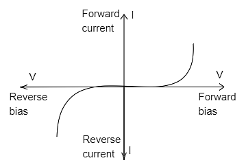
V-I Curve for P-N Junction Depicting Avalanche Breakdown Phenomenon
Also Read:
| Related Articles | ||
|---|---|---|
| Junction Transistor | Digital Electronics and Logic Gates | Extrinsic Semiconductors |
| Intrinsic Semiconductors | Bridge Rectifier | Application of Junction Diode |
Zener Breakdown
[Click Here for Sample Questions]
When a reverse-biassed voltage is supplied across the terminals of a highly doped PN junction diode, the depletion region begins to increase almost quickly. A significant number of carrier electrons and holes will be created due to this voltage. On one side of the depletion region are electrons, and on the other are holes. These charge carriers will aid in building a strong electric field across the junction of the diode. The applied reverse voltage determines the magnitude of the generated electric field - the magnitude of the induced electric field increases when the reverse-biassed voltage increases. The electrons in the valence band will feel a force from this electric field.
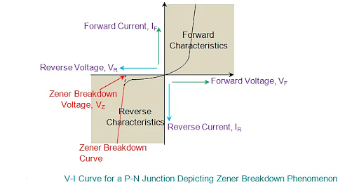
V-I Curve for P-N Junction Depicting Zener Breakdown Phenomenon
Zener vs Avalanche Breakdown: What's the Difference?
[Click Here for Sample Questions]
The difference between Zener and Avalanche breakdown is:
| Zener Breakdown | Avalanche Breakdown |
|---|---|
| It occurs because of a high electric field causing electrons in the valence band to come in the conductance band. | It occurs because of the collision of free atoms and electrons due to high electric field |
| The potential barrier doesn’t get destroyed. | The potential barrier gets destroyed. |
| The regions need to be highly doped for this. | The regions need to be lightly doped for this. |
| The voltage magnitude is relatively low. | The voltage magnitude is relatively high. |
| The VI curve has a sharper slope. | The VI curve is not as sharp as Zener breakdown |
| When temperature increases, its voltage decreases, so it has a negative temperature coefficient. | When temperature decreases, its voltage increases, so it has a positive temperature coefficient. |
| The flow of electrons across the p kind material barrier of the valence band to the evenly filled n-type material conduction band. | It is an occurrence of raising the flow of electric current or electrons in insulating material or semiconductor by giving the high voltage. |
| Its depletion region is thin. | Its depletion region is thick. |
| The electric field is strong. | The electric field is weak. |
| This breakdown generates electrons. | It generates holes as well as electrons. |
| Its reverse potential is low. | Its reverse potential is high. |
| Its ionisation is due to the electric field. | Its ionisation is due to the collision. |
Things to Remember
- The anode and cathode terminals are connected by a breakdown diode, which is a two-terminal electrical component. Diodes built of semiconductor objects such as Si (Silicon) and Ge (Germanium) are available in a variety of shapes and sizes.
- Zener breakdown occurs when a high electric field is created over a junction. Avalanche Breakdown, on the other hand, occurs in the device as a result of electrons colliding at a high rate.
- In an avalanche breakdown, the minority charge carriers in the semiconductor device that migrate across the depletion have kinetic energy. The value of this kinetic energy is proportional to the applied reverse voltage.
- The way the two diodes work is the most significant distinction between them. Zener breakdown happens when there is a high electric field across the junction. The phenomena of Avalanche Breakdown, on the other hand, is triggered by the collision of extremely fast-moving electrons.
- The key distinction between these two is that their mechanism occurs as a result of a high electric field and atoms colliding with flowing electrons. Both breakdowns may occur at the same time.
- The avalanche diode is built to endure avalanche breakdown without being destroyed by the rapid and drastically increased reverse current.
Also Read:
Sample Questions
Ques. Describe the Zener Diode. (2 marks)
Ans. The Zener Diode is a passive component that uses the Zener Breakdown principle to work. Clarence Zener created it in 1934, and it works in the same way as a standard diode in forward bias, enabling current to pass. The diode, on the other hand, only conducts when the applied voltage reaches the Zener Breakdown value in reverse bias conditions. Its function is to protect other semiconductor devices from transient voltage pulses. Its function is that of a voltage regulator. The Zener reverse breakdown is caused by electron quantum tunnelling caused by a high-intensity electric field.
Ques. Describe the process of Zener breakdown. (5 marks)
Ans. Because of their limited depletion region, highly doped p-n junction diodes experience Zener breakdown. The tiny depletion area provides a strong electric field when the reverse biassed voltage applied to the diode is raised. Because of their limited depletion region, highly doped p-n junction diodes experience Zener breakdown.
- When the reverse biassed voltage applied to the diode approaches Zener voltage, the electric field in the depletion area is strong enough to pull electrons from their valence band.
- Valence electrons that get enough energy from the strong electric field in the depletion area will break bonding with the parent atom. Valence electrons that have broken their bond with their parent atom are known as free electrons.
- Electric current is transported from one area to another by free electrons. The electric current is dramatically increased by a bit of increase in voltage at the Zener breakdown point.
- Zener breakdown occurs at low reverse voltage, but avalanche breakdown happens at high reverse voltage.
- Zener breakdown occurs because Zener diodes have a relatively small depletion zone. The breakdown area of a Zener diode is where it usually works. Zener breakdown occurs in Zener diodes with a voltage (Vz) less than 6V.
Ques. What is avalanche breakdown? (2 marks)
Ans. The free electrons in a PN junction device migrate over the depletion region. As a result, they have velocity, and these electrons will have kinetic energy. Because of covalent bonding, these electrons will clash with other stationary electrons firmly bound to the atom. This high current can create Avalanche Breakdown, which is the breakdown of a diode.
Ques. What will happen if the avalanche diode's reverse bias voltage is increased? (5 marks)
Ans. Suppose the reverse bias voltage provided to the avalanche diode is increased even more. In that case, the minority carriers (free electrons or holes) will gain a significant quantity of energy and be propelled to higher speeds. Free electrons colliding with atoms at fast speeds will transmit their power to the valence electrons.
- The valence electrons that obtain enough energy from the high-speed electrons will become free electrons and separate from the parent atom. These liberated electrons are accelerated once more.
- When the free electrons collide with other atoms again, more electrons are knocked off.
- A significant number of minority carriers (free electrons or holes) are formed due to this continual contact with the atoms. These high quantities of free electrons carry the diode's excess current.
- The junction breakdown or avalanche breakdown occurs when the reverse voltage applied to the avalanche diode grows.
- A minor increase in voltage will rapidly increase the electric current. This abrupt surge in electric current may irreversibly destroy the regular p-n junction diode.
- On the other hand, Avalanche diodes cannot be destroyed because they are specifically engineered to function in the avalanche breakdown region.
Ques. How can you say that Zener breakdown is a controllable phenomenon? (2 marks)
Ans. The quantity of charge carriers created may be effectively controlled by altering the electric field applied, making Zener break down a controllable phenomenon. The diode junction will typically break down below 5V due to Zener breakdown, but the device will not be damaged unless there is no way to escape the heat generated.
Ques. What is the definition of a breakdown diode? (2 marks)
Ans. The breakdown diode is a two-terminal electrical component connecting the anode and cathode terminals. Several sorts of diodes are available in the market, made with semiconductor objects, namely Si (Silicon) & Ge (Germanium). The diode's primary function is to enable current to flow in only one way while blocking current flow in the opposite direction.
Ques. What is a Zener Diode? (2 marks)
Ans. When a specific voltage is attained, the Zener diode incorporates an individual and heavily doped PN-junction, designed to work in the reverse bias direction. This diode has a reverse breakdown voltage for current conductivity and can operate continuously in reverse bias mode without being crushed.
Ques. Explain how temperature affects avalanche and Zener breakdowns. (2 marks)
Ans. When the electric field is substantially more robust, the electrons are dragged from the valence band to the conduction band, causing Zener breakdown. As the temperature rises, the band gap narrows, requiring a minor electric field to tear electrons from the valence to the conduction bands. As a result, the Zener breakdown voltage lowers as the temperature rises. As a result, the temperature coefficient of Zener breakdown is negative.
An avalanche breakdown occurs when a group of electrons knocks out another electron from the conduction band, resulting in an electron-hole pair. The oscillations of atoms increase as temperature rises, reducing the mean accessible route for electrons. As a result, the breakdown voltage rises as the temperature rises in avalanche breakdown. As a result, the temperature coefficient for avalanche breakup is positive.
Ques. What exactly is an avalanche diode? (2 marks)
Ans. The breakdown of an avalanche diode is meant to occur at a specific reverse bias voltage. This diode junction is primarily intended to prevent current concentration and thus diode damage during a breakdown. Avalanche diodes are used as support valves to control the system's pressure and avoid overvoltages. This diode, like the Zener diode, has a similar sign.
Ques. Describe the difference in the construction of the Zener diode and Avalanche diode. (3 marks)
Ans. Silicon or other semiconductor materials are used to make avalanche diodes. Although the construction of an avalanche diode is similar to that of a Zener diode, the doping level in an avalanche diode differs.
Zener diodes have a lot of doping. As a result, the depletion region of a Zener diode is exceptionally narrow. Reverse breakdown occurs at lower voltages in a Zener diode due to this thin depletion layer or area.
Avalanche diodes, on the other hand, are minimally doped. As a result, the depletion layer in an avalanche diode is much broader than in a Zener diode. In an avalanche diode, reverse breakdown occurs at higher voltages due to the broad depletion region. The breakdown voltage of an avalanche diode is carefully controlled during manufacture by regulating the doping level.
For Latest Updates on Upcoming Board Exams, Click Here: https://t.me/class_10_12_board_updates
Check-Out:



Comments