



Exams Prep Master
A transistor, which is used to amplify electrical signals, is a semiconductor device. In modern-day electronics transistors and semiconductor devices plays a major and important role. Transistor has basically two primary use cases one as an amplifier another as a switch. Transistors play an important role in different aspects of electronics such as in computers, audio devices, oscillators, etc. Generally, the low voltage DC is turned on or off by transistors in the mode of operation, which the concept behind the operation of a transistor as a switch relies on. Both PNP and NPN transistors can be used as switches. A basic terminal transistor can be operated differently from a signal amplifier by biasing both NPN and PNP bipolar transistors, and by an “ON / OFF” static switch. Here, we will be discussing transistors as switch amplifiers in detail along with some important questions.
| Table of Content |
Key Takeaways: Transistor, VI Characteristics, Switch, Amplifier, Circuit, Forward bias, Reverse bias, Oscillators, Voltage, Semiconductor device
What is a Transistor?
[Click Here for Sample Questions]
A transistor is consisting of three terminals. We call these three terminals:
Base – activation of the transistor is done by the base.
Emitter- it is the negative lead of the transistor.
Collector – It is called the positive lead of the transistor.

As the transistor is made of semiconductors, transistors can be of PNP transistors which is having the N-type material in between the two P-type materials, and NPN transistors which is having the P-type material in between the two N-type materials. Transistors are basic elements in integrated circuits.
The video below explains this:
Transistor Detailed Video Explanation:
Also Read:
| Related Articles | ||
|---|---|---|
| LC Oscillations | Transformers | Power in Alternating Current |
| Types of Transistors | Types of LED | Schottky Diode |
What does a Switch do?
[Click Here for Sample Questions]
A switch offers as an open circuit when it is off and offers as a short circuit when it is on. In other words, it can be said that a switch provides infinite resistance during its off condition and provides zero resistance during its own condition hence a switch can be imagined as an off controlled resistor that provides zero or infinite resistance to the circuit without an intermediate value.

A transistor on the other hand can be considered as a controlled resistance between emitter and collector. It is controlled by the current in the base-emitter junction by controlling the base-emitter current. The emitter-collector resistance can be made either nearly infinite or nearly zero. A transistor gives quite a large resistance to the circuit but it is not ideally infinite, also gives very small resistance but it is also not ideally zero.
Transistor Switch Working
[Click Here for Sample Questions]
In a transistor characteristic, there are three regions they are cut-off region, linear region, and saturation region. In the linear region for a wide range of collector-emitter voltage Vce, the collector current Ic remains constant as the voltage has a wide range and the collector current is almost constant. There will be significant power loss if the transistor is operated in this region but in a practical switch when it is off the voltage across it will be equal to open-circuit voltage. But the current is zero hence there is no power loss.
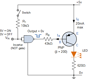
Similarly, when the switch is on, the current through the switch is as high as the short circuit current, but the voltage across the switch is zero. Hence there is no power loss again.
When we want a transistor to be operated as a switch it must be operated in such a way that the power loss during on and off conditions should be nearly zero or very low. It is only possible when the transistor is only operated in the marginal region of the characteristics there are two marginal regions in the characteristics of a transistor and these are the cut-off region and saturation region. When the base current is zero the collector current Ic will have a very small constant value for a wide range of collector-emitter voltage VCE. So, when the transistor is operated with a base current less or equal to zero the current through the collector to the emitter Ic is very tiny. Hence the transistor is said to be in off condition but at the same time, power loss across the transistor switch that is Ic into the VCE is negligible because of the very tiny collector current Ic. Hence the transistor is said to be operated as an off switch. Now suppose the transistor is connected in series with a load of resistance RL in normal conditions. The voltage across the load is PL. hence current through the load is Il = Vl/Rl.
If the transistor is operated with the base current Ib1 for which collector current is Ic1. If the load current Vl/Rl = Il which is also called as I out am less than Ic1 then the transistor is operated in the saturation region. Here for any current less than Ic1 through the transistor collector to emitter, there will be a very tiny collector-emitter voltage VCE. Hence in this situation, the current through the transistor is as high as load current but the voltage across the transistor VCE is quite low. Hence power loss in the transistor gain is negligible. The transistor behaves as a short circuit switch or on the switch. To make a transistor as a switch we should make sure that the applied base-emitter current must be high to keep the transistor in saturation region for a given load current.
What is an Amplifier?
[Click Here for Sample Questions]
The amplifier is a device. It is used to turn the low voltage signals from source equipment into a high voltage signal. Amplifiers are used to increase the power, current or voltage of a signal. These are mostly used in music equipment, electronics, computers, etc. it is a circuit that amplifies an input signal. It receives an input signal and increases that particular input signal strength as the output signal.

Transistor as an Amplifier
A transistor can be used as an amplifier, such that it takes to raise the strength of a weak signal to make it a strong signal. So, to understand this consider an NPN transistor having an emitter, base, and collector. Connect this transistor to an external circuit. Connect the circuit in such a way that the negative terminal is connected to the emitter and the positive terminal is connected to the collector. Due to this circuit, at the first junction emitter-base, it will become forward bias. Such that electrons from the emitter will cross the junction and reaches the base. This is due to the heavy doping of emitters.

Now in the second junction base and collector junction. The negative terminal of the circuit is connected to the P side and the positive terminal is connected to the N side. Such that it becomes a reverse-biased circuit. The width of the depletion layer will be more. so, no electrons will be able to cross the depletion layer and reach the collector. Electrons are trapped at the base itself. Crossing the depletion layer will become harder.
Due to this, there will be not much current flowing in the circuit. To make this transistor as an amplifier add an extra circuit to the existing circuit such that the negative terminal is connected to the emitter and the positive terminal is connected to the base. Due to this connection, the electrons in the emitter increase and move very faster. And also, the forward bias increases. Such that more and more electrons cross the first junction. And also making the base more positive increases the attraction of electrons by the positive terminal. So, the flow will increase. Due to this process, the depletion layer at the second junction decreases and it leads to more current flow in the circuit. In this way, for the smaller amount of the current, the output current will also be more. in this way, the transistor works as an amplifier.
Things to Remember
- To make a transistor as a switch we should make sure that the applied base-emitter current must be high to keep the transistor in saturation region for a given load current.
- In the cut-off region, the transistor acts as an open switch.
- In the saturation, the region transistor acts as a closed switch.
- In the saturation region, the depletion layer decreases by decreasing the emitter voltage drop.
- The base-emitter voltage in the saturation region is unpredictable.
Also Read:
Sample Questions
Ques: Difference between NPN and PNP transistors? (3 marks)
Ans:
| NPN Transistors | PNP Transistors |
|---|---|
| One P type semiconductor is kept between the two N type semiconductors | It is made in such a way that one N type material is kept between two P terminals. |
| The current flows from the collector terminal to the emitter terminal. | The current flows from the emitter to the collector terminal. |
| The current which is flowing from the collector is generated by keeping a positive voltage. | The current flow from the emitter to the collector is generated at the emitter terminal by keeping a positive voltage. |
| When the current is reduced in the base, the transistor doesn’t function across the collector terminal. | When the current is present at the base of a PNP transistor, then the transistor switches off. |
| With the more increase in the current in the base terminal, the transistor switches. | When there is no current flow at the base terminal the transistor switch. |
Ques: Why is the collector region wider than the emitter region in BJT? (2 marks)
Ans: In BJT collector region is wider and base region is thinner. The collector is made wider so as make heat dissipation easier whereas a thinner base will increase the value of β of the transistor.
Ques: Differentiate FET and BJT (3 marks)
Ans:
| FET | BJT |
|---|---|
| Unipolar device (that is current conduction by only one type of either electron or hole). | bipolar device (current conduction by both electron and hole). |
| High input impedance due to reverse bias. | Low input impedance due to forward bias. |
| Gain is characterized by transconductance | Gain is characterized by the voltage gain |
| Low noise level | High noise level |
Ques: In which region transistor acts as an open switch? (2 marks)
Ans: In the cut-off region both the junctions in the transistor are reverse biased. The transistor will have zero current in it because the emitter doesn’t release any charges to the base from it. Current is negligible in it. In this situation the transistor acts as an open switch.
Ques: In which region transistor behaves as a closed switch? (2 marks)
Ans: In the saturation, the region transistor acts as a closed switch. In this region, both the junctions in the transistor are forward biased. The negative terminal is connected to the emitter. Such that the collector current becomes free from base current. So, the transistor acts as a closed switch.
Ques: Define the different operating regions of the transistor. (3 marks)
Ans: The various operating regions of the transistor are
Active Region: It is defined as in which the transistor function is biased in reverse direction and emitter function in forwarding direction.
Cut-off Region: The region at which the collector and the emitter functions are reverse biased.
Saturation Region: The region at which the collector and emitter functions are forward biased.
Ques: What are the three types of configurations in transistors? (2 marks)
Ans: i) Common base configuration
ii) Common emitter configuration
iii) Common Collector-Configuration.
Ques: In a common base connection, IE = 1mA, IC = 0.95mA. Calculate the value of IB . (2 marks)
Ans: Ie = Ib + Ic
1 = Ib + 0.95
Ib = 0.05 mA
For Latest Updates on Upcoming Board Exams, Click Here: https://t.me/class_10_12_board_updates
Check-Out:



Comments