



Education Journalist | Study Abroad Lead
Diodes are two-terminal electronic components that conduct current in just one direction. A diode has high resistance on one end and low resistance on the other. Diodes are like a valve for an electrical circuit. The most common type of diode used is known as a semiconductor diode. It has a p–n junction associated with two electrical terminals.
| Table of Content |
Key Terms: Diode, Symbol of diode, semiconductor diode, two-terminal electronic, electricity, resistance, voltage
What is a Diode?
[Click Here for Sample Questions]
A diode is an electrical component with two terminals that conducts electricity mostly in one direction. On one end, it has a high resistance and low resistance on the other end.
- Diodes are used to protect the circuits by limiting the voltage in circuits as well as to convert AC to DC.
- They transfer electricity in the same direction but the manner in which they transfer electricity differs.
- Semiconductors like silicon and germanium are most commonly used to make diodes.
- Diodes come in a variety of shapes and sizes and have their own set of applications.
- Diodes consist of a warm cathode along with a plate, in which electrons only move a single way from the cathode to the plate.
Read More:
Symbol of Diode
[Click Here for Previous Year Questions]
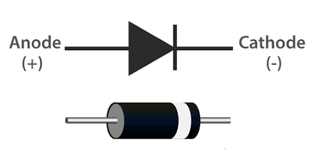
A diode consists of two terminals known as anode and cathode. The arrowhead represents the anode. The anode symbolizes the conventional current flow direction in the forward-biased condition. The vertical bar represents the cathode. The symbol for a typical diode is given in the figure below:
Construction of Diode
[Click Here for Sample Questions]
Diodes are formed from 2 semiconductor materials – silicon and germanium.
- A diode is considered to be forward-biased when the anode voltage is greater than the cathode voltage, and it conducts current readily with a minimal voltage drop.
- A diode is considered to be reverse-biased when the cathode voltage is higher than the anode voltage.
- The arrow in the symbol depicts the direction of conventional current flow when current flows through the diode.
Types of Diodes
[Click Here for Previous Year Questions]
There are many types of diodes available. Some of the widely used diodes are mentioned below:
- Light Emitting Diode
- PN Junction Diode
- Zener Diode
- Photodiode
- Schottky Diode
- Laser Diode
- Avalanche Diode
- Varactor Diode
- Tunnel Diode

Light Emitting Diode (LED)
Light is produced when an electric current between the electrodes passes through this diode.
- In other words, Light is produced when a sufficient quantity of forwarding current runs through it.
- This light is not visible in many diodes because the frequency levels are too low to allow visibility.
- Light Emitting Diodes are available in different colors.
- Tricolor LEDs are LEDs that can emit three colors at once.
- The energy gap of the semiconductor used in the diode determines the color of light.
P-N Junction Diode
P-N junction diodes are also referred to as rectifier diodes.
- These diodes are made of semiconductor material and are utilized in the rectification process.
- Two layers of semiconductors are used to make a P-N junction diode.
- P-type material is doped on one layer of the semiconductor material, while N-type material is doped on the other.
- The P-N junction is formed by the combination of both p-type and n-type layers. As a result, the diode is known as a P-N junction diode.
- The P-N junction diode permits the current to flow in forward direction but prevents it from flowing in the reverse direction.
Zener Diode
Zener diode is the most useful type of diode because it can offer a consistent reference voltage.
- These diodes are reverse biased and break down when a particular voltage is applied.
- A stable voltage is generated when the current traveling through the resistor is limited.
- In a power supply, Zener diodes are commonly employed to give a reference voltage.
Photo Diode
Even a small quantity of current flow caused by light can be detected by a photodiode.
- These are quite useful in detecting light.
- Photodiode is a reverse bias diode, which is commonly seen in solar cells and photometers.
- Photo Diodes are even utilized to generate electricity.
Schottky Diode
In Schottky diodes, forward voltage is lower than that of other silicon P-N junction diodes.
- When there is a low current and the voltage varies between 0.15 and 0.4 volts, a drop in the voltage can be seen.
- In order to achieve that performance, these are constructed differently.
- Schottky diodes are widely used in rectifier applications.
Laser Diode
Laser diode is a unique type of diode because it emits coherent light.
- It's found in a lot of CD players, DVD players, and laser printers.
- These are more expensive than LEDs but less expensive than other laser generators.
- The only disadvantage of these laser diodes is their short life.
Avalanche Diode
Avalanche diode is a reverse bias diode that uses the avalanche phenomenon to operate.
- The avalanche breaks down when the voltage drop is constant and it is independent of the current.
- They are utilized for photodetection because of their high sensitivity.
Varactor Diode
A varactor diode is a reverse-biased P-N junction diode with electrically variable capacitance. Varicaps, tuning diodes, voltage variable capacitor diodes, parametric diodes, and variable capacitor diodes are all terms used to describe these diodes.
Tunnel Diode
A tunnel diode (also known as an Esaki diode) exhibits practically negative resistance because of the quantum mechanical process known as tunneling.
- The PN junction in tunnel diodes is strongly doped and around 10 nm wide.
- Conduction band electron states on the n-side are more or less aligned with valence band hole states on the p-side, resulting in a broken bandgap.
Characteristics of a Diode
[Click Here for Sample Questions]
The main characteristics of a diode are:
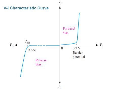
Forward Biased Diode
When the diode is forward-biased and the current is flowing, there is a minor voltage drop across it. The forward voltage for silicon diodes is 690mV, while the forward voltage for germanium diodes is 300mV. The potential energy across the p-type material is positive, while the potential energy across the n-type material is negative.
Reverse Biased Diode
A diode is said to be reverse-biased when the battery voltage is totally depleted. The reverse voltage for silicon diodes is -20μA, while the reverse voltage for germanium diodes is -50μA. The potential energy across the p-type material is negative, while the potential energy across the n-type material is positive.
Zero Biased Diode
If the voltage potential across the diode is zero, the diode is said to be zero-biased.
Applications of the Diode
[Click Here for Previous Year Questions]
Some of the basic applications of the Diode are mentioned below:
- Diodes in Reverse current protection
- Diodes in clamping circuits
- Diodes in logical gates
- Diodes in the clipping circuit
- Diodes as a rectifier
Things to Remember
- A diode is a two-terminal electronic component that conducts electricity in one direction.
- It has high resistance on one end and low resistance on the other end.
- In the symbol of a diode, the arrowhead represents the anode and the vertical bar represents the cathode.
- The anode represents the conventional current flow direction in the forward-biased condition toward the cathode.
- Diodes are commonly made up of only two semiconductor materials, Silicon and Germanium.
Also Read:
Previous Year Questions
|
Sample Questions
Ques: Which Diode is used in solar cells and photometers? (All India 2015, 1 Mark)
Ans: A photodiode is a p-n junction semiconductor device that transforms light into electricity. When photons are absorbed in the photodiode, electricity is formed. Optical filters, built-in lenses, and large or tiny surface areas can all be found in photodiodes. The common, traditional solar cell used to generate electric solar power is a large area photodiode.
Ques: Which semiconductor material is used for manufacturing Diodes? (All India 2016, 1 Mark)
Ans: Silicon and germanium are commonly used for the manufacturing of diodes.
Ques: .Draw the (i) symbol and (ii) the reverse I-V characteristics of a Zener diode. Explain briefly, which property of the characteristics enables us to use Zener diodes as a voltage regulator. (All India 2008 C, 2 Marks)
Ans: (i) 
(ii) 
The Zener diode is operated in the reverse breakdown region and the voltage across it remains constant due to this they are used as voltage regulators.
Ques: Draw the circuit diagram of an illuminated photodiode in reverse bias. Write the main use of the photodiode and Zener diode (Delhi 2010, 2 Marks)
Ans: Circuit diagram of Photodiode-

Photodiodes are used in the demodulation of optical signals and detection of the optical signals. Zener diodes are used as DC voltage regulators.
Ques: Name the device, D which is used as a voltage regulator in the given circuit and give its symbol. (Delhi 2011, 2 Marks)

Ans: The device D is a Zener Diode.
The Symbol of Zener diode is 
Ques: Explain, how a depletion region is formed in a junction diode? (Delhi 2011, 2 Marks)
Ans: With the formation of p-n junction, the holes from p-region diffuse into the n-region and electrons from n-region diffuse into p-region and electron-hole pairs combine and get annihilated.
This input produces a potential barrier, VB across the junction which opposes the further diffusion through the junction. Thus, a small region is formed in the vicinity of the junction, depleting free charge carriers. It has only immotile ions called the depletion region.
Ques: Draw the circuit diagram showing how a p-n junction diode is
(i)forward biased
(ii)reverse biased.
How is the width of the depletion layer affected in the two cases? (All India 2011 C, 2 Marks)
Ans: Circuit diagram of forward biased and reverse biased p-n junction diode is illustrated below:

First diagram illustrates the circuit diagram of forward biased p-n junction diodes and the second diagram illustrates the circuit diagram of reverse biased p-n junction diodes.
Ques: Explain with the help of a circuit diagram how a Zener diode works as a DC voltage regulator? Draw its I-V characteristics. (All India 2009, 3 Marks)
Ans: Zener diode is commonly used as voltage regulator.
Principle: Zener diode is operated in the reverse breakdown region. The voltage across it remains constant. The voltage is equal to the breakdown voltage for a high charge in reverse current.

Ques: With the help of a suitable diagram, explain the formation of depletion regions in a p-n junction. How does its width change when the junction is
(i)forward biased and
(ii)reverse biased? (All India 2009, 3 Marks)
Ans: When the p-n junction is formed, the holes from p-region diffuse into the n-region and electrons from n-region diffuse into p-region and electron-hole pairs combine and get annihilated.
This input produces a potential barrier, VB across the junction opposes the further diffusion through the junction. This small region formed in the vicinity of the junction which is depleted of free charge carriers and has only immotile ions is called the depletion region.
Circuit diagram of forward biased and reverse biased p-n junction diode is illustrated below:

(i) The width of the depletion layer decreases in forward bias.
(ii) The width of the depletion layer increases in reverse bias.
Ques: (i) Describe the working of Light Emitting Diodes (LEDs).
(ii) Which semiconductors are preferred to make LEDs and why?
(iii) Give two advantages of using LEDs over conventional incandescent low-power lamps. (All India 2011, 3 Marks)
Ans: (i) Working of LED: LED is a forward biased p-n junction diode. It converts electrical energy into optical energy of infrared and visible light.
It is always in forward bias. Due to this the thin depletion layer and low potential barrier facilitate the diffusion of electrons and hole through the junction when high-energy electrons of the conduction band combine with the low-energy holes in the valence band. The energy is released in the form of photons and can be seen in the form of light.
(ii) Semiconductors of suitable band gap (close to 1.5 eV) are preferred to make LED size GaAs, CdTe, etc. The other reasons to select these materials are high optical absorption, availability of raw material, and low cost
(iii) Uses of LEDs:
(a) LED can work at very low voltage and consume very less power in comparison to incandescent lamps
(b) They take very less time to operate and have a long life.
Ques: Draw the circuit diagram of a full-wave rectifier using p-n junction diode. Explain its working and show the output input waveforms. (Delhi 2012, 3 Marks)
Ans: The circuit diagram of full wave rectifier is shown below:

The input waveform and output waveform is given in the diagram below:

The working of the waveform is based on the principle that junction diodes offer very low resistance in forward bias direction and high resistance in reverse bias direction.
Ques: How is a Zener diode fabricated so as to make it a special purpose diode? Draw 7-V characteristics of Zener diode and explain the significance of breakdown voltage, (ii) Explain briefly, with the help of a circuit diagram, how a p-n junction diode works as a half-wave rectifier. (Delhi 2009C, 5 Marks)
Ans: (i) Zener diode works only in reverse breakdown region due to this it is considered as a special purpose semiconductor.

Reverse current is due to the flow of electrons from n-side to p-side and holes from p-side to n-side. The reverse biased voltage increases the electric field across the junction increases significantly and then reverse biased voltage V – Vz. After that the electric field strength is high enough to pull the electrons from p-side and accelerate it to n-side.
These electrons are responsible for the high current at the breakdown.

Voltage regulator converts an unregulated DC output of a rectifier into a constant regulated DC voltage, using Zener diodes. Thus, the voltage drop across RL increases without any change in the voltage drop across the Zener diode. This is because of the breakdown region, Zener voltage remains constant even though the current through the Zener diode changes.
When the input voltage decreases, the current through Rs and Zener diodes decreases. The voltage drop across Rs is reduced without any change in the voltage across the Zener diode.
Now, any change in input voltage results in the change in voltage drop across Rs. This change takes place without any change in voltage across the Zener diode. Thus, Zener diode acts as a voltage regulator.
(ii) Circuit diagram of p-n junction diode as a half-wave rectifier is illustrated below

Diode conducts corresponding to the positive half cycle and does not conduct during the negative half cycle. Hence, AC is converted by diode into unidirectional pulsating DC. This is also known as half-wave rectification.

Ques: (a) Explain with the help of a diagram, how a depletion layer and barrier potential are formed in a junction diode.
(b) Draw a circuit diagram of a full-wave rectifier. Explain its working and draw input and output waveforms. (Delhi 2014 C, 5 Marks)
Ans: (a) The formation of p-n junction takes place by the diffusion of charge. When the p-type semiconductor is joined with n-type semiconductor the diffusion of free charges across the junction starts.
Due to the formation of the p-n junction, the holes from p-region diffuse into the n-region, and electrons from n-region diffuse into p-region. The electron-hole pair combines and gets eliminated.
This input produces a potential barrier, VB across the junction which opposes the further diffusion through the junction. Thus, a small region that forms in the junction which is depleted of free charge carriers and has only immotile ions is called the depletion region.
Potential barrier: The potential distribution near the p-n junction is known as the potential barrier.

The circuit diagram of full wave rectifier is shown below:

The input waveform and output waveform is given in the diagram below:

The working of the waveform is based on the principle that junction diodes offer very low resistance in forward bias direction and high resistance in reverse bias direction.
Ques: Why is a Zener diode considered as a special purpose semiconductor diode? Draw the I-V characteristics of Zener diodes and explain briefly, how reverse current suddenly increases at the breakdown voltage? Describe briefly with the help of a circuit diagram, how a Zener diode work’s to obtain a constant DC voltage from the unregulated DC output of a rectifier. (Delhi 2009 C; Foreign 2012, 5 Marks)
Ans: Zener diode works in the reverse breakdown region which is why it is considered as a special purpose semiconductor.

Reverse current is due to the flow of electrons from n-side to p-side and holes from p-side to n-side. The reverse biased voltage increases the electric field across the junction increases significantly and then reverse biased voltage V – Vz. After that the electric field strength is high enough to pull the electrons from p-side and accelerate it to n-side.

Voltage regulator converts an unregulated DC output of a rectifier into a constant regulated DC voltage, using Zener diodes. Thus, the voltage drop across RL increases without any change in the voltage drop across the Zener diode. This is because of the breakdown region, Zener voltage remains constant even though the current through the Zener diode changes.
When the input voltage decreases, the current through Rs and Zener diodes decreases. The voltage drop across Rs is reduced without any change in the voltage across the Zener diode.
Now, any change in input voltage results in the change in voltage drop across Rs. This change takes place without any change in voltage across the Zener diode. Thus, the Zener diode acts as a voltage regulator.
For Latest Updates on Upcoming Board Exams, Click Here: https://t.me/class_10_12_board_updates
Also Read:



Comments