



Education Journalist | Study Abroad Lead
Pin diode is mainly made of p-type and n-type materials which were sandwiched with an Intrinsic layer in between the p and n-type materials. Any diode is a thermionic valve having two electrodes (an anode and a cathode which are the p and n-type materials). The center layer does not allow the current to flow through it because it behaves as an insulator. Every diode has a vast application in its respective domain likewise the PIN diode is mainly used in high voltage rectifiers, RF switches, microwave switches, variable attenuators, etc. Generally, every diode act as a one-way valve for the flow of current, and the Pin diode can also be used in the same way to stop the flow of current after a relative increase in voltage or current flow is observed. In this article, we will look at Pin diode and its applications along with the input and output characteristics.
| Table of Contents |
Key takeaways: PIN diode, Photodiode, Rf switches, High Voltage Regulators, regulators, p-n diodes, semiconductor, p-type semiconductor, n-type semiconductor
What is Pin diode?
[Click Here for Sample Questions]
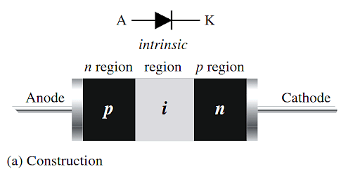
Pin diode is a diode with an undoped intrinsic semiconductor material that is placed in between the p-type semiconductor and an n-type semiconductor region. The p-type and n-type regions are typically heavily doped in comparison to the intrinsic region in the junction. These PIN diodes are wider than the normal p-n diodes and the end terminals were used for ohmic contacts.

Pin Diode
This wider intrinsic region makes the PIN diode a special diode for different types of applications in contrast to the normal p-n junctions. This diode when placed in a circuit, is assumed to be a resistor due to the wider intrinsic layer which offers a constant resistance to the flow of current.
-
Structure of Pin Diode
The structure of pin diode is normally cylindrical in which all the three layers were sandwiched and a plastic hosing is applied on the entire diode leaving two ohmic contacts for the connection in the circuit. The holes are the majority charge carriers in the P-type material and the electrons are the majority charge carriers in the N-type material in the structure of the PIN diode.

Structure of Pin Diode
Also Read:
Invention
[Click Here for Sample Questions]
The PIN photodiode was invented by Jun-ichi Nishizawa along with his colleagues in the late 1950s. It is an alternative for PN-junction for particular applications. After the PN-junction diode, which was developed in the 1940s, the diode was first used as a high-power rectifier with low frequency in electric circuits.
It is known that the occurrence of an intrinsic layer in between the p-n junction significantly increases the breakdown voltage for the detection of high-voltage. It also provides high voltage applications where the radio and microwaves can be realized. The name was called a PIN diode because of the arrangement inside the diode in which the P-type material, Intrinsic layer, N-type material were placed in sequential order.

Pin Diode
Working principle
[Click Here for Sample Questions]
When the PIN diode is unbiased, the charge carriers will flow from the N-type region to the intrinsic region due to the concentration of the charge carriers in a certain region. Therefore, the width of the depletion region increases at the N-I junction. Hence, width is more towards the N-side and less towards the I-side.
Working Principle of Pin Diode
The reason for this is that N-type material is highly doped while the Intrinsic layer is not so heavily doped. Hence, when charge carriers (electron are the majority carriers on N-side) flow from N-type to the Intrinsic layer, it creates a depletion region, but the width of the depletion region on either side of the N-I junction will be different.
Input and Output characteristics
[Click Here for Sample Questions]
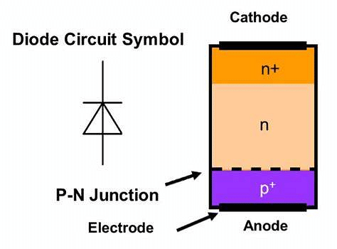
Pin Diode has a wider junction when compared to any other typical diodes. This wider area enhances the pin diode to have low capacitance when connected in reverse-biased mode. The depletion region here generated here is much wider and the size of the region remains almost constant with high variation of biasing voltage.
During the forward biasing, the charge carriers move into the depletion region and as soon as the holes and electrons come closer, the current flow will start.
During the reverse biasing condition, the intrinsic layer among the P & N layers increases the gap between the two layers and reduces the capacitance of the diode. This results in isolation of the diode.

Applications
[Click Here for Sample Questions]
The main applications include Rf (radio frequency) switches, voltage rectifiers, microwave switches, Variable attenuators, photodiodes.
- As RF switches and microwave frequency switches, pin diode behaves as voltage variable resistors and it is capable to give much higher levels of consistency than RF relays that are frequently the only other alternative diodes.
- As a voltage rectifier, the intrinsic layer in the diode generates a separation between both the layers, allowing higher reverse voltages to be withheld by the layers in the diode. It is placed where the device works on high voltages.
- As a variable attenuator, all the major applications were based on the feature of the diode being used as a voltage variable resistor. Three diodes can be used to replace the fixed resistors of the π circuit to create a variable attenuator, and such circuits have been described for circuits.
- In the form of a photodiode, it converts light into the form of current in the depletion region of the photodiode. When the depletion region increases by inserting the intrinsic layer, the performance is also increased as there is an increase in the volume of light change.
Diode Circuit Symbol
Advantages and disadvantages of Pin Diode
[Click Here for Sample Questions]
The advantages of pin diode are:
- A very low reverse bias voltage is required
- High quantum efficiency
- A larger bandwidth can be obtained
- Lower noise performance and high efficiency and economical than other diodes
- The wider depletion region provides more area of working.
- Vast resistance (tolerance) to the increase in reverse voltages.
Symbol of Pin Diode
The disadvantages of pin diode are:
- The main disadvantage is that it cannot amplify the signal passed through this.
- Low sensitivity and varies with the temperature changes.
- Very high complicated packing which when misplaced without accuracy will cause malfunctioning of the PIN diode.
- The recovery time after a power loss is much greater when compared to a typical diode.
Things to Remember
- Pin diode is similar to the typical p-n junction diode with the only difference being the intrinsic layer midway of the diode.
- When the PIN diode is subjected to forward bias, the depletion region at the p-n junction reduces and the current starts flowing through the diode.
- When the PIN diode is set to reverse biased condition, the area of the depletion region widens.
- At a smaller reverse bias voltage, the depletion layer completely vanishes.
- During the low biased condition, pin diode will show less capacitance and the width of the intrinsic area also widens.
- PIN diode has wide applications only because of the intrinsic layer.
Also Read:
Sample Questions
Ques: How the pin diode can be used as a photodetector? (3 marks)
Ans: When light falls on pin photodiode, reverse current flows through the photodiode which is proportional to the intensity of the light. The intensity depends on the wavelength of the light. Incident light is converted to electric energy, so they are used as optical detectors. At very low frequency it absorbs a high amount of energy with the relation with its intensity and hence the pin diode can be used as the photodiodes as it responds to the light very specifically and accurately.
Ques: What are the applications of pin diode? (3 marks)
Ans: Some applications of pin diode are:
- They are intensively used in optical communication systems.
- They can be seen in the research field of nuclear radiation detectors and radiation alarms.
- They are sensitive to electromagnetic radiation and can detect their limitations.
Ques: Give examples of practical pin diodes present in the industry and the main characteristics of the PIN diode? (3 marks)
Ans: SFH203 and BPW34 are the general-purpose PIN diodes in a 5 mm clear plastic case and their bandwidth is over 100 MHz.
Their main characteristics are:
- Low Capacitance
- High breakdown voltage
- Sensitive to photodetection
- Charge carriers’ storage
Ques: What is the role of the intrinsic layer in the PIN diode? (3 marks)
Ans: The main role of the intrinsic layer in a diode is to increase the gap between the two ohmic conductors (the P-type and the N-type materials). Hence the capacitance between both the regions can also be reduced as this behaves as a non-conducting resistance.
Hence the isolation will be increased between the ohmic conductors and hence enhances and progress the performance of the general diode by changing the volume of the space where the light will fall and causes the photo effect and the Presence of light can be easily detected.
Ques: Why should one use pin diodes for RF Switching? (5 marks)
Ans: Pin diodes are used for RF switching as:
- When the PIN diode is used at the radio and microwave frequencies, it behaves as a current-controlled resistor.
- During the forward biasing, It allows the current and the RF energy to flow in the forward direction.
- When at reverse biasing condition, it blocks the current and the RF energy at a time and provides higher resistance.

The above diagram depicts the forward and the reverse bias behavior of the pin diode.
- In general, the PIN diodes give very good linearity and can be used for very higher frequency and greater power applications.
- But a large amount of DC power is needed for biasing and hence can be used as a radio frequency switch.
- Hence by using this PIN diode as the main component in the RF circuits they can be easily detected and used as the RF switches.
Ques: Mention the structural details of the PIN diode? (5 marks)
Ans: The structure of pin diode can be described as:
- In pin diode, the intrinsic semiconductor is sandwiched between the high doped P and the high doped N regions.
- These pin diodes will show a very small switching time. Because of the intrinsic layer.
- Due to the high resistivity possessed by the intrinsic layer, there is a smaller switching time.
- Due to the increase in the depletion region, the covalent bonds are broken and the surface area for photosensitivity is therefore increased.
- This property of photosensitivity is used in fields of light sensors, artificial retina systems, and many more.
- The entire structure is covered with a plastic hose to cover it from the external effects.
Ques: Describe the disadvantages of PIN diode? (5 marks)
Ans: The following are the disadvantages of the PIN diode:
- The main disadvantage is that it cannot amplify the signal passed through this and has a lesser active area in the diode’s internal region
- Very high complicated packing which when misplaced without accuracy will cause malfunctioning of the PIN diode.
- The recovery time after a power loss is much greater when compared to a typical diode.
- It has low sensitivity and varies with the temperature changes.
- The response time is a bit slower when compared to the typical PN diode.
- The area spread will be lesser due to the cylindrical arrangement.
- Pin diode is used in the circuits in larger numbers and can not be used wholly in the circuit arrangement.
- If it loses the connection with the circuit, then the entire communication is lost and must be immediately replaced without any repairs.
For Latest Updates on Upcoming Board Exams, Click Here: https://t.me/class_10_12_board_updates
Also Read:



Comments