



Education Journalist | Study Abroad Lead
V-I characteristics or a current-voltage characteristic, also known as a curve (current-voltage curve). It is a relationship between the electric current flowing through a circuit, apparatus, or substance and the associated voltage. It is often represented in a chart or graph, where voltage(v) is measured along the x-axis and current(I) is measured along the y-axis.
The V-I graph provides useful information regarding resistance and deconstructs an electronic component. It also reveals a device's functioning area.
| Table of Content |
Key Terms: V-I Characteristics, Current, Voltage, Graphical Curves, Circuit, Resistance, Liner, Non- Liner, SCR, MOSFET, LED, P-N Junction Diode
What do V-I Characteristics mean?
[Click Here for Sample Questions]
The I-V Characteristic of an electrical device or element is a set of graphical curves used to define the behavior of the device or component inside an electrical circuit.
This graph is obtained when current is measured via an electronic component as a voltage is put across it.
It is the relationship between the voltage and the electric current flowing through a circuit, device, or substance.
Voltage(v) is measured along the x-axis, while the current(I) is measured along the y-axis, as seen in a chart or graph,as it's easier to change the applied voltage than it is to change the current.
V-I characteristics are based on Ohm's law, which states that the potential difference (voltage) across a component increases, so does the current.
The precise relationship between voltage and current varies depending on the component which can be depicted on an I-V graph.
Also Read:
| Related Articles | ||
|---|---|---|
| Rectifier | Full Wave Rectifier | Half Wave Rectifier |
| Types of Transistors | Types of LED | Schottky Diode |
Uses of V-I Characteristics
[Click Here for Sample Questions]
I-V characteristic curves are frequently used:
- to identify and analyze the fundamental properties of a component or device,
- to mathematically represent its behavior inside an electrical circuit.
- to represent the numerous values.
- It displays a family or group of curves on the same graph as most electronic devices have an endless number of I-V characteristic curves representing the various inputs or parameters.
- The V-I graph gives valuable data regarding resistance and deconstructs an electronic component.
- It also specifies a component's working range.
- We may learn where and how to utilize a component in an electric circuit by examining these features.
- A useful tool for determining a device's or component's functional capabilities by exhibiting its various current and voltage combinations.
- It also acts as a visual aid for seeing what is happening within a circuit.
Types of V-I Characteristics
[Click Here for Sample Questions]
Some of the VI characteristics are Liner, Non-Liner, SCR, MOSFET, LED, PN Junction Diode.
Linear V-I Characteristics
- Resistance is constant.
- The V-I curve will be a straight line going through the origin when we plot this graph.
- A linear characteristic of an electrical component is found only in a specific region.
- A diode is the best example.
Non-linear V-I Characteristics
-
The resistance of a circuit component is not constant throughout.
- Resistance is a function of voltage or current, it has a non-linear characteristic.
- For example, the resistance of a diode varies depending on the voltage applied.
- However, for a short transmission zone, it has a linear feature.
V-I Characteristics of SCR
[Click Here for Sample Questions]
V-I Characteristics of SCR (Silicon Controlled Rectifier)is a graphical representation of current through the SCR and voltage across the anode to cathode terminal.
SCRs are three-terminal semiconductor switching devices that are used to manage power flow rectification, regulation, and inversion.
An SCR has three primary modes of operation, based on the examination of its V-I characteristics: reverse blocking mode, forward blocking mode, and forward conduction mode. The SCR is also known as a thyristor or a thyrode transistor.
V-I Characteristics of MOSFET
[Click Here for Sample Questions]
MOSFET means Metal Oxide Semiconductor Field Effect Transistor.
It is a three-terminal device in which the voltage output controls current flow between the output terminals, source, and drain.So they have terminals like drain (D), source (S), and gate (G), with a substrate (S) as the fourth terminal.
Depletion type transistor, Enhancement type transistor are the two types of power MOSFET
V-I Characteristics of LED
[Click Here for Sample Questions]
- The "Light Emitting Diode," or LED stands for light-emitting diode, and it is a strongly developed forward-driven p-n junction that converts electric energy into optical energy.
- The shorter lead is for the n or cathode side, whereas the longer lead is for the p or cathode side.
- Gallium arsenide is used to make the connection.
- When light is forward biased, photons are emitted from the non-metallized surface of the n area to the p region and from the p region to the n region.
- Free carrier density at the junction rises.
- Excess secondary electrons join with free carriers on either side.
- Photons are emitted as energy during recombination.
- Emitted photons have energies that are equal to or slightly less than the bandgap.
- As current grows in the forward bias, the intensity of light increases until it hits a maximum, and further increases in current decrease the intensity of light.
V-I Characteristics of PN Junction Diode
[Click Here for Sample Questions]
When an N-type material is fused with the P-type material to create a semiconductor diode, it is known as a PN junction diode.
The circuit connection for determining the V-I characteristics of a PN junction diode is shown in the figure below.
The graph below is showing V-I characteristics curve of the p-n junction diode
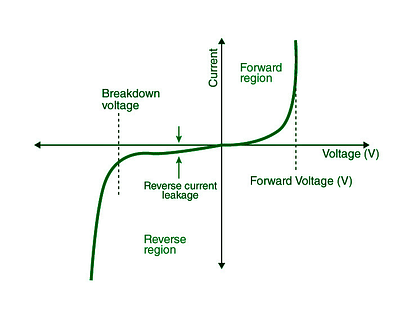
We can observe from the graph that the diode acts in three separate locations, which are:
- Zero bias
- Forward bias
- Reverse bias
When the p-n junction diode is at zero bias, no external voltage is applied, implying that the potential barrier at the junction precludes current passage.
When the p-n junction diode is in forwarding bias, the positive terminal of the external voltage is connected to the p-type, and the negative terminal is connected to the n-type. When the diode is positioned in this manner, the potential barrier is lowered. Potential barriers fall and current flows when the voltage is 0.7 V for silicon diodes and 0.3 V for germanium diodes.
While the diode is in forwarding bias, the current develops slowly, and the curve that forms is non-linear as the voltage applied to the diode overcomes the potential barrier. The diode acts normally once it has overcome the potential barrier, and the curve climbs rapidly as the external voltage rises, creating a linear curve.
The p-type is connected to the negative terminal of the external voltage while the PN junction diode is under negative bias, whereas the n-type is connected to the positive terminal. As a result, the potential barrier has increased. At first, reverse saturation current arises because minority carriers are present at the junction.
Things to Remember
- V-I characteristics curve is a relationship between the electric current flowing through a circuit, apparatus, or substance and the associated voltage.
- This graph is obtained when current is measured via an electronic component as a voltage is put across it.
- Voltage(v) is measured along the x-axis, while the current(I) is measured along the y-axis, as seen in a chart or graph,as it's easier to change the applied voltage than it is to change the current.
- I-V characteristic curves are frequently used to identify and analyze the fundamental properties of a component or device, to mathematically represent its behavior inside an electrical circuit, to represent the numerous values, and so on.
- VI characteristics are SCR, MOSFET, LED, PN Junction Diode,Zener diode.
- The "Light Emitting Diode," or LED stands for light-emitting diode, and it is a strongly developed forward-driven p-n junction that converts electrical energy into optical energy.
- V-I characteristics curve of the p-n junction diode acts in three separate locations, which are, Zero bias, Forward bias, Reverse bias
Also Read:
Sample Questions
Ques: Two electrical components, X and Y, are depicted with their I–V characteristics. Which of the following statements is correct? (2 marks)
A) As the current increases, the resistance of X increases.
B) At 2 V, the resistance of X is half that of Y.
C) X is a resistor, while Y is a semiconductor diode.
D) Y is a filament light, while X is a resistor.
ANS. C is the correct answer. X is a linear I-V graph. This indicates that the graph's gradient is constant. As a result, I/V and resistance are both constant (because gradient = 1/R). This is the I-V graph for a constant temperature conductor, such as a resistor. The I-V graph Y begins with a gradient of zero and rapidly climbs. This means it has infinite resistance at first, then progressively reduces. This describes a device that only allows current to flow in one way, such as a semiconductor diode.
As a result, the solution is C.
Ques: Name the semiconductor device that can be used to regulate a dc power source that isn't regulated. Explain the functioning principle of this gadget using the I-V characteristics. (2 marks)
ANS. The zener diode is a device that is used to regulate an unregulated dc power source.
Principle of operation: When a zener diode is used in the reverse break down area, the voltage across it remains nearly constant (equivalent to the break down voltage V-I) despite a considerable variation in the reverse current.
Ques: What are the most common PN junction diode applications? (3 marks)
ANS. PN junction diode applications are applied in the following :
- The diode is used in LED lighting applications when it is forward-biased.
- In many electric circuits, PN junction diodes can also be utilised as rectifiers.
- In various industry-related machines as a voltage-controlled oscillator.
- It's found in most modern radars.
- As circuits for detectors and demodulators.
- In digital logic designs and circuits, as a switch.
- In the clamping circuits of a television receiver.
- Amplification and voltage multiplier circuits.
Ques: The V-I characteristic of a semiconductor diode is depicted in the diagram below. (3 marks)
1) Determine the semiconductor diode that was used.
2) Create a circuit schematic to achieve the device's specified characteristic.
3) Describe how this diode can be used as a voltage regulator in a few words.
ANS: (I) A Zener diode is employed as a semiconductor diode.
(iii) A voltage regulator using a zener diodeWhen a zener diode is operated in the reverse breakdown zone, the voltage across it is nearly constant (equal to the breakdown voltage Vz) despite a substantial shift in reverse current. As the input voltage rises, the current flowing through RS and the zener diode rises as well. This raises the voltage drop across RS while leaving the voltage across the zener diode same. This is because, even though the current through the zener diode changes, the zener voltage remains constant in the breakdown area. Similarly, if the input voltage drops, the voltage across RS drops, but the voltage across the zener diode stays the same.
As a result, any change in the input voltage causes a change in the voltage drop across RS but no change in the voltage across the zener diode. As a result, the zener diode is a voltage regulator.
Ques: Explain concisely, using appropriate illustrations, the forward and reverse biasing of a p-n junction diode. Draw their typical curves in both circumstances.. (2 marks)
ANS: The battery is connected to the silicon diode through a potentiometer (or rheostat), allowing the applied voltage to be varied while noting the associated current values.
We analyse the variation of current with applied voltage using the circuit designs shown in figs. I and (ii) to derive the V-I characteristics.
The V-I characteristics of a junction diode show that it only permits current to pass when it is forward biased. When an alternate voltage is put across the diode, current flows only during the forward biased portion of the cycle.
For Latest Updates on Upcoming Board Exams, Click Here: https://t.me/class_10_12_board_updates
Check-Out:



Comments