



Education Journalist | Study Abroad Lead
Characteristics of a transistor can be determined from the graph showing relation between the current and the voltage of any transistor and any configuration. The transistor circuit configurations are of three types namely – Common Emitter Transistor, Common Base Transistor and Common Collector Transistor.
| Table of Contents |
Key Terms: Semiconductors, Transistors, Current, Emitter, Collector, Voltage, Base terminals, Collector terminals, Resistance
What is a Transistor?
[Click Here for Sample Questions]
A transistor is a three-terminal device that contains a base, emitter and collector. In a common-emitter configuration, the input voltage is applied between emitter and base terminals and the output voltage is applied across the emitter and collector terminals.

Transistor
The video below explains this:
Transistor Detailed Video Explanation:
Also Read:
| Related Articles | ||
|---|---|---|
| Full Wave Rectifier | Energy Bands | Rectifier |
| Zener Diode | Bridge Rectifier | Application of Junction Diode |
Input Characteristics of a Transistor
[Click Here for Sample Questions]
The input characteristics of a transistor is obtained between the input current (IB) and input voltage (VB) when the output voltage VCE is constant.
We can examine the input current values at each point by keeping the output voltage VCE constant and changing the input voltage VBE at different points.
Use the values obtained from different points and plot the values of IB and VBE at constant VCE to draw a graph.
At a constant VCE
Rin = VBE/IB
You can calculate the input resistance Rin using the above equation.

Input Characteristics for CE Configuration
Output Characteristics of a Transistor
[Click Here for Sample Questions]
The common emitter’s output characteristic is obtained between the output voltage VCE and output current IC when the input current IB is constant. We can examine the values of collector IC at each point by keeping the base current IB constant and changing the output voltage VCE at different points.
To get the output characteristics of a common emitter configuration, plot a graph between IC and VCE.
At a constant IB
Rout = VCE/IC
You can calculate the output resistance Rout using the above equation.

Output Characteristics of a Transistor
Configurations of a Transistor
[Click Here for Sample Questions]
Using the three types of configuration can be used to design any transistor circuit. The three types of configuration of a transistor are:
- Common Emitter Transistor
- Common Base Transistor
- Common Collector Transistor
Common Emitter (CE) Configuration of a Transistor
In Common Emitter Configuration, the transistor’s emitter terminal will be connected common between the output terminal and the input terminal.
| Transistor Characteristics | Definition | Formula/Expression | Characteristic Curve |
|---|---|---|---|
| Input Characteristics | Variation of emitter current (IB) with Base-Emitter voltage (VBE) when Collector-Emitter voltage (VCE) is held constant. | Rin = ΔVBE/ΔIB | VCE = Constant | |
| Output Characteristics | Variation of collector current (IC) with Collector-Emitter voltage (VCE) when the base current (IB) is held constant. | Rout = ΔVCE/ΔIC | IB = Constant |  |
| Current Transfer Characteristics | The variation of the collector current (IC) with the base current (IB) when the collector-emitter voltage (VCE) is constant. | α = ΔIC/ΔIB | VCB = Constant |  |
Common Base (CB) Configuration of a Transistor
In Common Base Configuration, the transistor’s base terminal will be connected common between the output terminal and the input terminal.
| Transistor Characteristics | Definition | Formula/Expression | Characteristic Curve |
|---|---|---|---|
| Input Characteristics | Variation of emitter current (IE) with Base-Emitter voltage (VBE) when the Collector Base voltage (VCB) is held constant. | Rin = ΔVBE/ΔIE | VCB = Constant |  |
| Output Characteristics | Variation of collector current (IC) with Collector-Base voltage (VCB) when the emitter current (IE) is held constant. | Rout = ΔVCB/ΔIB | IE = Constant | |
| Current Transfer Characteristics | The variation of the collector current (IC) with the emitter current (IE) when the Collector Base voltage (VCB) is constant. | α = ΔIC/ΔIE | VCB = Constant |  |
Common Collector (CC) Configuration of a Transistor
In Common Collector Configuration, the transistor’s collector terminal will be connected common between the output terminal and the input terminal.
| Transistor Characteristics | Definition | Characteristic Curve |
|---|---|---|
| Input Characteristics | Variation of emitter current (IB) with Collector-Base voltage (VCB) when the Collector Base voltage (VCB) is held constant. | 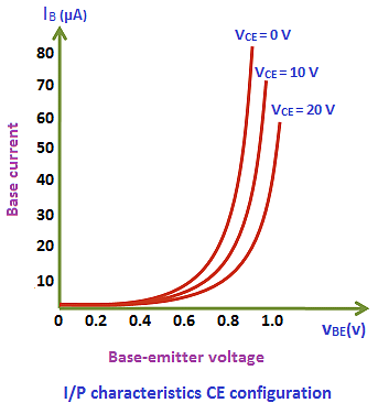 |
| Output Characteristics | Variation of emitter current (IE) with Collector-Emitter voltage (VCE) when the base current (IB) is held constant. |  |
| Current Transfer Characteristics | The variation of the collector current (IE) with the base current (IB) when the Collector-Emitter voltage (VCE) is constant. |  |
Relationship between Two Current Gains
[Click Here for Sample Questions]
Current gain (α) = IC/IE
Current gain (β) = IC/IB
And, Collector current IC =αIE = βIB
One of the three circuit configurations is used in this configuration. The input and output impedance values are average. Also, the current and voltage gains are average. This configuration’s output signal has a phase shift of 180?, indicating that the input and the output are inversely proportional to each other.
Things to Remember
- Characteristics of a transistor are plots that represent the relationships between the current and the voltages of a transistor in a particular configuration. The transistor configuration circuits can be analyzed using characteristic-curves.
- Input Characteristics: These determine the changes in input current. They also show the variation in the values of input voltage, wherein the output voltage is constant.
- Output Characteristics: These are a plot of output current against the output voltage with constant input current.
- Current Transfer Characteristics: These characteristics curve shows the variation of output current in accordance with the input current. Here, the output voltage is kept constant.
- The transistors with characteristic frequency (fT) less than or equal to 3 MHZ are called low-frequency transistors.
- Transistors with fT higher than or equal to 30MHZ are called high-frequency transistors.
- Transistors with fT more than 3 MHZ and transistors less than 30 MHZ are called intermediate frequency transistors.
Also Read:
Sample Questions
Ques. Define common base configuration in the transistor. (1 Mark)
Ans. In Common Base Configuration, the transistor’s base terminal is connected common between the output terminal and the input terminal.
Ques. Name the different configurations of a transistor. (2 Marks)
Ans. There are three configurations of a transistor namely:
- Common Emitter (CE)
- Common Base (CB)
- Common Collector (CC)
Ques. Calculate the value of IB in a common base connection, when IE = 1mA, IC = 0.95mA. (2 Marks)
Ans. Using the equation:
IE = IB + IC
1 = IB + 0.95
IB = 1 - 0.95
= 0.05mA
Ques. Find out the value of base current in a common base connection when the current amplification factor is 0.9 and the emitter current is 1mA. (3 Marks)
Ans. Here, α = 0.9 and IE = 1mA
α = IC/IE
Or, IC = αIE
= 0.9 x 1
= 0.9mA
Also, IE = IB + IC
Base current, IB = IE - IC
= 1 - 0.9
= 0.1mA
Ques. What are the formulas for calculating the following terms? (3 Marks)
a) Input resistance (ri)
b) Output resistance (ro)
c) Current amplification factor (β)
Ans. a) Input Resistance (ri)
ri = (ΔVEB/ΔIB)VCE = constant
b) Output Resistance (ro)
ro = (ΔVCE/ΔIC)IB = constant
c) Current Amplification Factor (β)
β = (ΔIC/ΔIB)VCE = constant
Ques. Draw the transfer characteristic curve of a base biased transistor in CE configuration. Explain clearly how the active region of the VD versus V, curve in a transistor is used as an amplifier. (3 Marks) [Delhi 2011]
Ans. For using the transistor as an amplifier we will use the active region of the V0 vs. V, curve. The slope of the linear part of the curve represents the rate of change of the output with input. It is negative, that is why as input voltage of the CE amplifier increases its output voltage decreases and the output is said to be out of phase with input.

Ques. Draw typical output characteristics of an n-p-n transistor in CE configuration. Show how these characteristics can be used to determine output resistance. (4 Marks) [All India 2013]
Ans. Typical output characteristic curves :

Output Resistance, r0 =\((\frac {\bigtriangleup V_{CE}}{AI_c})_{I_B}\)

The reciprocal of the slope of the linear part of the output characteristic gives the value of output resistance (r0). The output resistance of the transistor is mainly controlled by the base-collector junction. The high magnitude of the output resistance (of the order of 100 K?) is due to the reverse biased state of this diode. This also explains why the resistance at the initial part of the characteristic, when the transistor is in saturation, is very low.
Ques. Give a circuit diagram of a common emitter amplifier using an n-p-n transistor. Draw the input and output waveforms of the signal. Write the expression for its voltage gain. (5 Marks) [All India 2009]
Ans. (i) (a) Common emitter configuration of n-p-n transistor

(ii) Transistor as an amplifier (C.E. configuration) : The circuit diagram of a common emitter amplifier using n-p-n transistor is given below :

The input (base-emitter) circuit is forward biased and the output circuit (collector- emitter) is reverse biased.
When no a.c. signal is applied, the potential difference VCC between the collector and emitter is given by
VCC = VCE + ICRC
When an a.c. signal is fed to the input circuit, the forward bias increases during the positive half cycle of the input. This results in an increase in IC and decreases in VCC. Thus during the positive half cycle of the input, the collector becomes less positive.
During the negative half cycle of the input, the forward bias is decreased resulting in decrease in IE and hence IC. Thus VCC would increase making the collector more positive. Hence in a common-emitter amplifier, the output voltage is 180° out of phase with the input voltage.

For Latest Updates on Upcoming Board Exams, Click Here: https://t.me/class_10_12_board_updates
Do Check Out:



Comments