



Education Journalist | Study Abroad Lead
Semiconductor devices are materials which have conductivity between conductors and Insulators. Devices that allow electric current to flow through them at certain conditions like heat, light or voltage are known as semiconductors. Semiconductor devices are widely used owing to their low-cost, compact configuration, and reliability. They are hence used in devices like sensors and emitters due to their ability to withstand a wide range of current and voltage ratings.
| Table of Content |
Key Terms: Semiconductors, Conductors, Insulators, Diodes, Transistors, Two-terminal, Three- terminal, Amplifier, Capacitor, Resistor, Voltage, Current, Electric current
What is a Semiconductor?
[Click Here for Sample Questions]
Semiconductors are materials which are:
- Not a good conductor
- Not a good insulator
- But conduct more electricity when heat, light, or voltage is applied.
Some of the examples of semiconductors are Selenium, Germanium, Silicon, Tellurium, Gallium arsenide. The current ratings of semiconductors ranges from 10-9 Amperes to voltage and ampere ratings greater than 5000, sometimes even extending to 100,000 volts. Semiconductor devices are microelectronic circuits that are complex in structure making them the prominent component of a vast majority of electrical and electronic devices in fields of communication, data-processing and industrial process control systems.
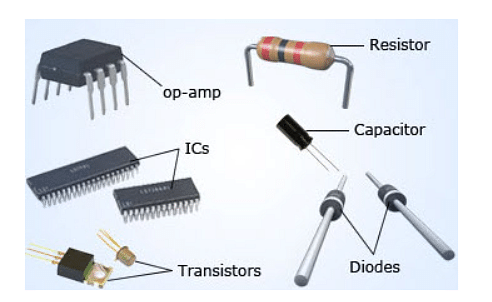
Semiconductor Device Examples
The video below explains this:
Semiconductors and Insulators Detailed Video Explanation:
Read More:
Types of Semiconductor Devices
[Click Here for Previous Year Questions]
Semiconductor devices are braodly categorised based on the number of terminals on the elctronic devices as follows:
Two-Terminal Semiconductors
These are semiconductor materials, which come with only one positive-negative (p-n) junction.
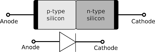
Two-Terminal Semiconductor Schematic
Three-Terminal Semiconductors
These semiconductor materials possess a positive-negative-positive (p-n-p) junction.
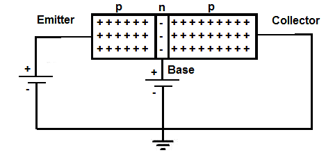
Three-Terminal Semiconductor Schematic
Some of the devices that uses the two types of semiconductors are tabulated below:
| Mass | Volume |
|---|---|
| Light-emitting diode (LED) | TRIAC |
| Phototransistor | Field-Effect Transistor |
| Tunnel Diode | Bipolar transistor |
| Laser Diode | Thyristor |
| Schottky Diode | Silicon Controlled Rectifier (SCR) |
| Zener Diode | Injunction Transistor |
The following are some of the types of semiconductor devices based the number of terminals:
Operational Amplifier (op-amps)
An operational amplifier, which is an integrated circuit, may boost a weak electric signal. There are two input pins and one output pin. The difference in voltage between the two input pins is amplified and sent to the output.

Operational Amplifier
Resistors
A resistor is a passive electrical component with two terminals that implement electrical resistance. Resistors are employed in electronic circuits for a variety of purposes, including reducing current flow, adjusting signal levels, dividing voltages, influencing active devices, and ending transmission lines. The different types of resistors are:
- Fixed Resistors
- Variable Resistors
- Thermistors
- Varistors
- Photoresistors
- Magneto Resistors
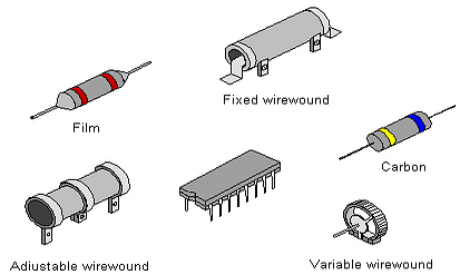
Resistors are used in street lighting, laptop and mobile chargers, temperature control, fan speed controller, measuring electrical current, temperature sensor, in-circuit functioning, etc.
Capacitors
In an electric field, a capacitor acts as a storage device for electrical energy. It is a passive electrical component with two terminals. Some of the applications of capacitor in daily life are as follows:

- In the ceiling fan, two capacitors are connected in a parallel series.
- Capacitors are also employed at utility substations to counterbalance the inductive loads introduced by transmission lines.
- The conditioning of the power supply is an essential application for capacitors. When charged, capacitors enable AC signals to pass but block DC signals.
Diodes
A semiconductor device with a single p-n junction is known as a diode. P-n junctions are typically created by fusing p-type and n-type semiconductor materials together. Electrons diffuse from the n-type region to the p-type region because the n-type region has more electrons and the p-type region has more holes. As a result, this phenomenon is used to manufacture light devices.

Transistors
A transistor is a device that functions as a switch or gate for electronic signals and regulates current or voltage flow. Transistors comprise three layers of semiconductor material, each of which may transport current.
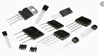
Transistors
Transistors come in two types:
- Bipolar junction
- Field effect
The development of two p-n junctions in two distinct configurations, such as n-p-n or p-n-p, results in the bipolar junction transistor. The three regions formed in this sort of transistor are known as the emitter, collector, and base or middle region. The field-effect transistor operates on the principle of conductivity, which can be changed by an electric field.
Semiconductor Electronics Class 12 Important Notes PDF
Semiconductor Electronics Class 12 Important Notes




Advantages of Semiconductors
[Click Here for Sample Questions]
- Because of their dependability, compactness, and low cost, semiconductor devices are widely used in many applications.
- A semiconductor is a distinct component that is utilised in optical sensors, power devices, light emitters, and solid-state lasers.
- Electronic circuits made of semiconductor devices are simple to design and inexpensive to manufacture.
- They have no filament and hence no power is required to cause electron emission.
- Semiconductors become operational as soon as the circuit is switched on.
- No humming noise is produced during operation.
- Semiconductor devices are shock proof in nature.
Applications of Semiconductor Devices
[Click Here for Previous Year Questions]
Devices based on semiconductor technology are extensively used in a wide range of electronic applications. Few examples are cited of how it may be used:
- Semiconductor devices are safe to use in electrical appliances that require a high voltage.
- Semiconductor materials are extremely useful in designing amplifiers and oscillators.

Semiconductors as Amplifiers
- Transistors (a semiconductor) are major elements in electronic components, such as microprocessors.
- Semiconductors are used in building logic gates and various forms of digital circuits.

Logic Gates
Important Topics for JEE MainAs per JEE Main;2024 Session 1, important topics included in the chapter Semiconductor Electronics are as follows:
Some important memory based questions from JEE Main 2024 Session 1 are given below: 1.In a given voltage regulator circuit, the reverse breakdown voltage of the Zener diode is 3V. Find the current through the Zener diode. (Circuit diagram was given.) 2. Find the current through the Zener diode if its breakdown voltage is 5 V. (Diagram was given.) |
Things to Remember
[Click Here for Sample Questions]
- Semiconductor devices are those materials which have conductivity between conductors and Insulators.
- Semiconductors allow electric current to flow only at certain conditions.
- A transistor functions as a switch or gate for electronic signals, regulating current or voltage flow.
- Semiconductors are classified into two terminal semiconductors and three terminal semiconductors.
- A resistor is a passive electrical component with two terminals that implement electrical resistance.
- A semiconductor device with a single p-n junction is known as a diode.
- A capacitor acts as a storage device for electrical energy.
Also Check Out:
Previous Year Questions
- Determine the type of gate. [JIPMER 2019]
- Which Logic gate is represented by the truth table? [JKCET 2012]
- Calculate ß when the emitter current is changed. [JEE Main 2021]
- What is the impurity atom to be doped for p type semiconductors? [JEE Advanced 1988]
- What is pure silicon. [JIPMER 2018]
- What is an intrinsic semiconductor. [MET 2012]
- Device that acts as a complete electronic circuit. [NEET 2010]
- Which have negative coefficient of resistance. [NEET 2020]
- Determine the logic gate? [NEET 2010]
- Determine the semiconductor device type. [NEET 1998]
- When is an npn transistor used as an amplifier. [NEET 1996]
- What causes increase in width of depletion region. [NEET 2020]
- A p-n junction diode is also used as? [NEET 1999]
- The value of photo electromotive force is proportional to? [NEET 2005]
- Which is p-type semiconductor? [NEET 2013]
- Calculate the voltage gain and power of the amplifier. [NEET 2017]
- The electrical network is equivalent to? [NEET 2017]
- The pn junction is forward biased when? [NEET 1988]
- At absolute zero, Si acts as? [NEET 1988]
- Calculate the power gain of the amplifier. [NEET 2010]
Sample Questions
Ques. Why are semiconductors so important? (2 marks)
Ans. It is important because of its two inbuilt properties:
- Can control the number of charge carriers (electrons and holes) and current flow can be controlled.
- Can give a unidirectional flow of current.
Ques. Name the semiconductor device that can be used to regulate an unregulated DC power supply. With the help of 7-V characteristics of this device, explain its working principle. (CBSE 2011) (2 marks)
Ans. Zener diodes are used as voltage regulators.
Principle: Zener diode is operated in the reverse breakdown region. The voltage across it remains constant, equal to the breakdown voltage for large charge in reverse current

Ques. Is it safe to use semiconductors in humans? (2 marks)
Ans. The semiconductor industry has a comparatively low rate of physical accidents. Since 1972, the semiconductor industry has been ranked in the top 5% of all U.S. companies for workplace health and safety.
Ques. What are the current applications of semiconductors? (2 marks)
Ans. Semiconductors are employed as temperature sensors in air conditioners, for example. Semiconductors are used in a wide range of digital consumer items, including mobile phones / Smartphone, digital cameras, televisions, washing machines, refrigerators, and LED bulbs.
Ques. Name the important processes that occur during the formation of a p-n junction. Explain briefly, with the help of a suitable diagram, how a p-n junction is formed.Define the term ‘barrier potential’? (CBSE 2011) (3 marks)
Ans.

During formation of the p-n junction, diffusion of charge takes place. As soon as p-type semiconductor is joined with n-type semiconductor, diffusion of free charges across the junction starts.
For explanation of formation p-n junction
With the formation of p-n junction, the holes from p-region diffuse into the n-region and electrons from n-region diffuse into p-region and electron-hole pairs combine and get annihilated.
This input produces a potential barrier, VB across the junction which opposes the further diffusion through the junction. Thus, a small region that forms in the vicinity of the junction which is depleted of free charge carriers and has only immotile ions is called the depletion region.
Potential barrier The potential distribution near the p-n junction is known as potential barrier
Ques.Carbon and silicon both have four valence electrons each, then how are they distinguished? (CBSE 2011) (2 marks)
Ans. The four valence electrons of carbon are present in the second orbit while that of silicon in the third orbit. So, energy required to extricate an electron from silicon is much smaller than carbon.
Therefore, the number of free electrons for conduction in silicon is significant, unlike carbon. This makes silicon conductivity much higher than carbon. This is the main distinguishable property.
Ques. Give two advantages of LEDs over the conventional incandescent lamps.(CBSE 2011) (3 marks)
Ans. When we apply sufficient voltage to the LED, electrons move across the junction into the p-region and get attracted to the holes there. Thus, electrons and holes recombine. During each recombination, the electric potential energy is converted into the electromagnetic energy and a photon of light with a characteristic frequency is emitted, this is how, LED works.
Advantages of LEDs over incandescent lamps
(i) Since, LEDs do not have a filament that can burn out, hence, they last longer.
(ii) They do not get hot during use.

Ques. What is required to manufacture semiconductors? (2 marks)
Ans. Silicon, germanium, and other pure elements are commonly used to make it. Impurities are added to the element to make semiconductors. The type and intensity of the additional impurities determine the element's conductance or inductance. Semiconductors are divided into two categories.
Ques. Draw energy band diagram of n-type and p-type semiconductor at temperature T > OK. Mark the donor and acceptor energy level with their energies. (CBSE 2014) (2 marks)
Ans.

For Latest Updates on Upcoming Board Exams, Click Here:https://t.me/class_10_12_board_updates
Also Check:



Comments