



Education Journalist | Study Abroad Lead
Transistor is a semiconductor device that is often used for amplifying or switching electronic signals and electronic powers. Transistors come in many shapes and sizes.
- Transistors are small electronic components with two main functions.
- A transistor acts as a switch to on and off electricity as well as amplifies signals.
- Small and low-power transistors are enclosed in a resin case to help protect the internal parts.
- A transistor can be defined as a miniature device used to control or regulate the flow of electronic signals.
Transistors are considered one of the major components of most electronic devices today. The transistor was developed in the year 1947 by three American physicists John Bardeen, Walter Brattain and William Shockley.
- Base: Activate the transistor
- Collector: The positive lead of the transistor
- Emitter: The negative lead of the transistor
| Table of Content |
Key Terms: Amplifier, Transistor, Semiconductor Diode, Insulator, Voltage, FET, BJT, Schottky transistor, Inverted-T Field-effect Transistor (ITFET), MOSFET
What is a Transistor?
[Click Here for Sample Questions]
A transistor is a semiconductor device that can be used for both conducting and insulating electric current or voltage.
- A transistor acts as a switch and an amplifier.
- It is a miniature device used to control or regulate the flow of electronic signals.
- Transistors are the key components in most of the electronic devices present today.
- Transistors were developed in 1947 by three American physicists John Bardeen, Walter Brattain and William Shockley.
- A transistor acts as a switch to on and off electricity as well as amplifies signals.
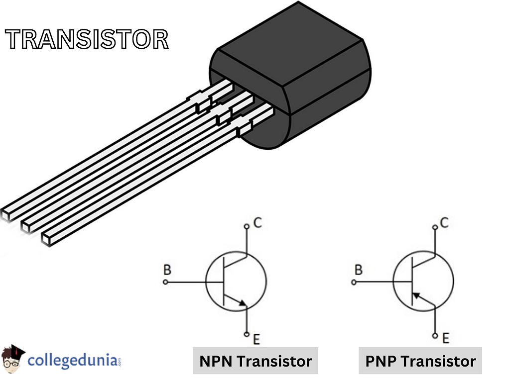
Transistor
Transistor as Switch
A switch should have on and off characteristics and to control it we need to give input to it as yes or no, 0 or 1, up or down.
- And since, a transistor has the collector, the base, and the emitter which means if the switch is “on” the current flows from the collector to the emitter.
- Input to the switch can be given through the base.
- If the base is given with 1, the switch is on. If the base is given with 0, the switch is off.
Transistor as Amplifier
A Transistor can be said to be a current booster.
- It takes in a very small weak signal through the base junction and the amplified signal will come out at the collector.
- The n-type material has electrons in abundance; the p-type material has holes that attract electrons.
- When the transistor is in its off state the holes in the base prevent electrons from flowing from the emitter to the collector.
- The transistor starts operating when holes start moving across the n-p junction.
- So when we supply a small positive signal at the base and make the emitter negatively charged and the collector positively charged, electrons are driven from the emitter to the base to the collector and take the transistor to its “on” state.
- So, the small-signal supplied to the base causes a big current to flow from emitter to the collector, thus amplifying.
The video below explains this:
Transistor Detailed Video Explanation:
Read More:
| Concept-Related Topics | ||
|---|---|---|
| Feedback Amplifier and Transistor Oscillator | Laser Diode | Pin Diode |
| Schottky Diode | Spintronics | Varactor Diode |
Transistors Working
[Click Here for Previous Year Questions]
A Bipolar Junction Transistor (BJT) comprises of three terminals (Emitter, Base and Collector). A BJT is a current-driven device wherein the two P-N junctions can be found within a BJT.
- One P-N junction is in between the emitter and base, while the second junction is in between the collector and base.
- A small amount of current flow is found to pass via the emitter to the base.
- It can control a large amount of current flow via the device from emitter to collector.
- As per the operation of BJT, the base-emitter junction is forward-biased, while the base-collector junction is in reverse-biased condition.
- When current is flowing via the base-emitter junction, a current is going to flow in the collector circuit.
To express the working of transistors, an example of an NPN transistor can be considered.
Operation of NPN Transistor
The NPN device emitter is composed of an n-type material, thus the majority of carriers are electrons.
- When the base-emitter junction has been forward-biased, the electrons shift from the n-type region toward the p-type region.
- The minority carrier holes shift towards the n-type region.
- When they both meet, they combine and allow current to flow across the junction.
- However, if the junction is reverse-biased, then the holes and electrons shift away from the junction.
- It thus creates a depletion region between the two areas, allowing no current to flow through them.
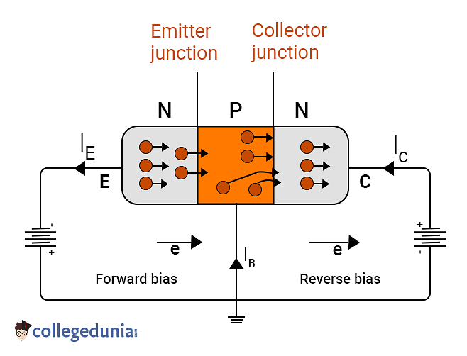
Operation of NPN Transistor
- When the flow of current is between the base and emitter, the electrons tend to exit the emitter and flow into the base.
- The electrons, typically, combine when they reach the depletion region.
- However, the doping in this region is low, with the base being very thin.
- This causes the electrons to be able to travel across the region without recombining with the holes.
- Thus, the electrons drift towards the collector.
In this way, the electrons flow across the reverse-biased junction while the current flows in the collector circuit.
Types of Transistors
[Click Here for Sample Questions]
There is a variety of transistors including, Schottky transistor, MOSFET, inverted-T field-effect transistor (ITFET), JFET, thin-film transistor, insulated-gate bipolar transistor, high electron mobility transistor, fast-reverse epitaxial diode field-effect transistor (FREDFET), tunnel field-effect transistor, organic field-effect transistor (OFET), diffusion transistor, and more. Some of the most important types of transistors are:
Power Transistor
These types of transistors are used to make high-power amplifiers and power supplies.
Bipolar Junction Transistor (BJT)
It is a device in which the current flows between two terminals which are the collector and emitter. BJT is known for its current control. They are used for the amplification of signals, high-voltage switches, and digital circuits.
- P-N-P Transistor: PNP transistors are a type of Bipolar Junction Transistor (BJT) wherein one n-type material is placed between two p-type materials. In this type of configuration, the device is going to control the current flow. PNP transistor is a 2-crystal diode connected in series. Both the right side and left side of the diodes are called the collector-base diode and emitter-base diode, respectively.
- N-P-N Transistor: NPN transistor is a type of transistor wherein the p-type material is found between two n-type materials. It is utilised to amplify weak signals to strong signals. In an NPN transistor, the electrons are seen to shift from the emitter to the collector, thus resulting in the building of current in the transistor.
There are three different types of configuration, which are the Common Base (CB), Common Collector (CC) and Common Emitter (CE).
Common Base (CB)
A Common Base configuration is a configuration where the base terminal of the transistor is common between input and output terminals.
Common Collector (CC)
In a Common Collector configuration, the collector terminals are observed to be common between the input and output terminals.
Common Emitter (CE)
In this type of configuration, the emitter terminal is common between the input and the output terminals.

CB, CC and CE Configurations
Small Signal Transistor
Small Signal Transistors are transistors that are used to amplify low-level signals but can also be used as a switch. Typical FE values for small signal transistors range from 10 to 500, with maximum ratings from about 80 to 600mA. This is useful in amplifiers, medical equipment, and measuring devices.
Switching Transistor
Switching transistors operate fully off or fully on. They are used in designing power supplies, electronic switches, and automation equipment.
Phototransistor
A phototransistor is an electronic switching and current amplification component which relies on exposure to light to operate. Since transistors are made from semi-conductive materials grown into crystals such as germanium or silicon, all transistors react to light. Phototransistors are used extensively to detect light pulses and convert them into digital electrical signals. These are operated by light rather than electric current.
Field-effect Transistor
A field-effect transistor is a transistor in which the voltage on one terminal creates a field that allows or disallows conduction between the other two terminals. It uses an electric field to control the flow of current in a semiconductor. The three terminals in a FET is Gate, Source and Drain.
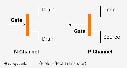
Field Effect Transistor (FET)
The voltage present at the gate terminal is able to control the current between the source and the drain. FET is considered to be a unipolar transistor wherein N-channel FET or P-channel FET is utilised for conduction. The primary applications of FETs are found in low-noise amplifiers, buffer amplifiers and analogue switches.
Darlington Transistor
A Darlington transistor is an electronics component made via the combination of two BJT connected in such a way that it allows a very high amount of current gain. Darlington has two transistors joined together. They are useful for amplification and used to make pre-amplifiers for audio.
High-frequency Transistor
High-frequency transistors are used in high-frequency ranges like radio, communication equipment, television signal, and microwaves.
Unijunction Transistor
They are a three-lead electronic semiconductor devices with only one junction that acts exclusively as an electrically controlled switch.
Metal Oxide Semiconductor FET
These are the transistors that are very important for logic circuit boards and computers. They are semiconductor devices that are widely used for switching purposes.
Characteristics of Transistors
[Click Here for Previous Year Questions]
The Characteristics of the transistor are the plots that help show the relationship between the current and the voltage of a transistor in a certain configuration. The types of characteristics are:
Input Characteristics
It helps to give the details about the change in input current, along with the variation in input voltage by retaining the output voltage to be constant.
- CB Configuration: Variation of emitter current, IE with base – Emitter voltage, VBE by holding the collector voltage to be constant, VCB.
- CC Configuration: Variation in IB as per VCB with collector-emitter voltage VCE constant.
- CE Configuration: Variation in IB as per VBE with VCE constant.

Input Characteristics
Output Characteristics
Output characteristics are a plot of the output current along with the output voltage by holding the input current to be constant.
- CB Configuration: Variation of collector current, IC along with VCB by holding the emitter current IE to be constant.
- CC Configuration: Variation in IE against the changes in VCE while IB is constant.
- CE Configuration: Variation in IC with changes in VCE while IB is constant.

Output Characteristics
Current transfer Characteristics
It shows the variation of the output current with the input current by holding the voltage to be constant.
- CB Configuration: Variation of IC with IE while VCB is constant.
- CC Configuration: This shows the variation of IE with IB when VCE is constant.
- CE Configuration: Variation of IC with IB while VCE is constant.

Current transfer Characteristics
Applications of Transistors
[Click Here for Sample Questions]
The applications of a transistor are:
- Transistors are used for making memory chips.
- Transistors are used for making most of the parts of modern electronic devices like smartphones, smartwatches, etc.
- It is used for Microprocessors and Microcontrollers
- When a large current or voltage is needed to be controlled, the Darlington transistor can be used.
- Transistor switches can be used to switch and control lamps, relays, or even motors.
Terminals of Transistors
[Click Here for Previous Year Questions]
There are three parts of a transistor includes:
- Collector
- Base
- Emitter
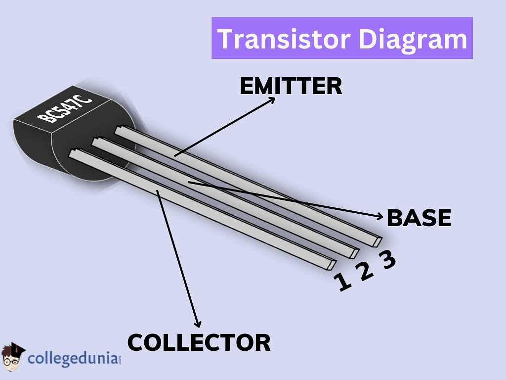
Transistor Diagram
The transistor contains three pins which are labeled as E, B, and C. Herein, E, B, and C in a transistor stands for the Emitter, Base, and Collector. The pin of the transistor is an emitter, the middle is the base and the right side is the collector. However, not all transistors use this configuration which means that these configurations might be different for some transistors.
Transistor Formula
[Click Here for Sample Questions]
The formula of transistors are given below:
For the NPN transistor, the emitter current is the total of base and collector current.
i.e., IE = IC + IB
For the PNP transistor, the collector current is the difference between the emitter current and the base current.
i.e., IC = IE - IB
Advantages of TransistorThe advantages of transistors include:
Disadvantages of TransistorsTransistors also have many disadvantages. They are:
|
Read More:
Things to Remember
- Transistor is made from silicon or germanium and it acts as an amplifier or a switch.
- A transistor has three leads, which are base lead, collector lead, and emitter lead.
- One of the primary advantages of a transistor is that it can develop better efficiency circuits.
- One of the disadvantages of a transistor is that It lacks a higher electron mobility.
-
There are three different types of configuration, the Common Base (CB), Common Collector (CC) and Common Emitter (CE).
Previous Year Questions
- In the depletion region of an unbiased…..[AMUEEE 2007]
- Pure silicon at 300 K has equal electron…...[AMUEEE 2009]
- The intrinsic carrier concentration of silicon sample…..[JKCET 2018]
- When a p−n junction diode is connected in forward bias its barrier potential [JKCET 2008]
- Which of the following truth tables corresponds to NAND gate.[AMUEEE 2011]
- In the figures shown below….[EAMCET 2010]
- Consider the following statements A and B…..[EAMCET 2003]
- To get an OR gate from a NAND gate, we need…..[VITEEE 2013]
- The decimal number equivalent to a binary number 1011001 is [WBJEE 2012]
- The output Y of the logic circuit shown in figure is best represented as [VITEEE 2014]
Sample Questions
Ques. Do Field-Effect Transistors have high input impedances? (1 Mark)
Ans. Field-Effect transistors come with high input impedances, ranging from a few mega ohms (M) to very high values.
Ques. How does the transistor work in a light bulb? (1 Mark)
Ans. The light bulb when connected to the battery illuminates the light automatically without the option to light the bulb only when it’s required so this is where the transistor comes in. The transistor helps in manually controlling the light so that it can be on when the light is needed and off when it is not required.
Ques. How do you explain the voltage gain of a Transistor? (1 Mark)
Ans. The voltage gained by a transistor can be stated as the ratio of amplified output to the supplied input. In other words, the gain of voltage in a transistor is always the ratio of the input to the output current.
Ques. Why Does Power Dissipation Occur Mainly in the Collector Junction? (1 Mark)
Ans. Since the collector junction is reverse-biased which means it offers more resistance to the flow of current, due to which a huge voltage drop occurs at the collector junction. That’s why power dissipation occurs in the collector junction.
Ques. Explain the importance of Transistor action. (1 Mark)
Ans. A transistor is a semiconductor device that is used for controlling, amplifying, and generating electrical signals. Without the use of a transistor, any of the above operations cannot be accomplished. Inside a transistor, there are millions of active components of integrated circuits. We call them microchips as they serve all kinds of required functions.
Ques: The AC current of a given transistor has a gain of 120. Determine the change in collector current in a transistor with a base current of 100 μA. (All India 2006, 2 Marks)
Ans: As per the given question,
- β = 120 ,
Δ IB = 100μA
Current gain:
β =Δ IC/Δ IB
Thus, when the VCE = constant
120= ΔIC/100μA
⇒ ΔlC = 120 × 100μA
= 12mA.
Ques. How does a transistor work? (2 Marks)
Ans. A transistor works when the electrons and the holes start moving across the two junctions between the n-type and p-type silicon. The small current that we turn on at the base makes a big current flow between the emitter and the collector.
So a very small amount of current flows through the emitter to the base which can control a reasonably large amount of current that flows through the device from emitter to collector. So the base current switches the whole transistor on and off.
Ques. Why is the MOSFET transistor attached to a heat sink in a component with a high current flow? (3 Marks)
Ans. Inside the DC Bench power supply there are some MOSFET transistors that are attached to a very large heat sink. Without the heat sink, the component quickly reaches 45o Celsius or 113 degrees Fahrenheit with a current of just 1.2A. And as a result, they will become much hotter as the current increases.
Whereas for an electric circuit with small currents we can just use resin body transistors that do not require a heat sink. Small and low-power transistors are enclosed in a resin case to help protect the internal parts. But higher power transistors will have a partly metal case which is used to help remove the heat which is generated as this will damage the component over time.
Ques. What are the advantages and disadvantages of a transistor? (5 Marks)
Ans. The advantages and disadvantages of a transistor are:
Advantages:
- It is small in size
- It is lower in cost
- It has an extremely long life span
- Transistor has a low operating voltage
- A better efficiency circuit can be developed with the help of a transistor
- No power consumption
- It has smaller mechanical sensitivity
Disadvantages:
- It is affected by cosmic rays and radiation
- It has a lower power dissipation
- It has a lower input impedance
- It is sensitive to temperature
- It produces very low energy
- It lacks higher electron mobility
- It can be easily damaged when electrical and thermal events arise
Ques. Write the difference between Bipolar Junction transistor Vs Field Effect Transistor. (5 Marks)
Ans. Bipolar Junction transistor Vs Field Effect Transistor:-
| Bipolar Junction Transistor | Field-effect Transistor |
|---|---|
| Medium noise generation | Low noise generation |
| Low current gain | High current gain |
| The offset voltage is required | No offset voltage is required |
| Low output impedance | High output impedance |
| High voltage gain | Low voltage gain |
| Low input impedance | Very High input impedance |
| Consumption of power is more | Consumption of power is less |
| Known for current control | Known for voltage control |
For Latest Updates on Upcoming Board Exams, Click Here: https://t.me/class_10_12_board_updates
Check-Out:



Comments