



Education Journalist | Study Abroad Lead
The difference between NPN and PNP transistors is mainly indicated by the flow of current. In the PNP transistor, the flow of current is in the inward direction whereas, in the NPN transistor, the flow of current is in the outward direction.
| Table of Content |
Keyterms: Transistor, Current, PNP transistor, NPN transistor, Voltage, Bipolar Junction Transistor, Semiconductors, Electrons
Transistor
[Click Here for Sample Questions]
Transistor is a semiconductor device that exchanges or transfers a weak signal from a sink resistance circuit to one. It regulates, methodizes, and amplifies electrical signals such as current or voltage.
These are special because they permit you to control the flow that flows through the circuit. Transistors control the flow of current by regulating and controlling the voltage between two of the leads. Every transistor has 3 leads.
The video below explains this:
Transistor Detailed Video Explanation:
Also Read:
| Related Articles | ||
|---|---|---|
| Electromagnetic Induction | Faraday’s Law of Electromagnetic Induction | Lenz’s Law and Conservation of Energy |
| Energy Consideration: A Quantitative Study | Eddy Currents | Inductance |
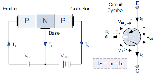
NPN Transistor
[Click Here for Sample Questions]
- NPN transistor is a type of Bipolar Junction Transistor.
- In this, electrons are major current carriers, and minor ones are holes.
- Their arrangement is in such a way that N-type doped semiconductors are separated by the layer of P-type doped semiconductors which is a thin layer material embedded between them.
- Emitter Current = Collector Current + Base Current

NPN Transistor
PNP Transistor
[Click Here for Sample Questions]
- PNP transistor is also a type of Bipolar Junction Transistor.
- In these, holes are the major source that carries current, and electrons are minor.
- Their arrangement is in a way that P-type doped semiconductor is separated by N-type doped semiconductor material which is a thin layer.
- Emitter Current = Collector Current + Base Current

PNP Transistor
Difference between NPN And PNP Transistors
[Click Here for Sample Questions]
| NPN Transistors | PNP Transistors |
|---|---|
| Two N-type layers are separated by one P-type thin layer. | Two P-type doped semiconductors are separated by N-type doped semiconductor material which is a thin layer. |
| NPN- Negative Positive and Negative | PNP- Positive Negative and Positive |
| It switches ON when electrons enter the base. | It switches ON when holes enter into the base. |
| The direction of Current is from Collector to Emitter | The direction of Current is from Emitter to Collector |
| It improves and unfolds because of the diverse positions of electrons. | It arises because of the flow of electrons. |
| The switching time is very fast. | The switching time in it is very Slow |
| The majority of charge carriers are Electrons. | The majority of charge carriers are Holes. |
| The minority of charge carriers are Holes. | The minority of charge carriers are Electrons |
| Emitter base junction | Emitter base junction |
| Collector Terminal | Emitter Terminal |
| The direction of current is from Emitter to Base | The direction of current is from Base to Emitter |
| Collector base junction | Collector base junction |
| Ground signal is Low. | Ground signal is High |
Working Difference between NPN And PNP Transistor
[Click Here for Sample Questions]
| Features | NPN Transistor | PNP Transistor |
|---|---|---|
| Biasing | Forward Bias- N-type emitter is connected to the negative pole and P-type emitter is connected to the positive pole of the same battery VEE. Reverse Bias- P-type base is connected to the negative pole and N-type emitter is connected to the positive pole of the same battery VCC. | Forward Bias- P-type emitter is connected to the positive pole and N-type emitter is connected to the negative pole of the same battery VEE Reverse Bias- N-type base is connected to the positive pole and the P-type base is connected to the negative pole of the same battery VCC |
| Current | Emitter current IE, Collector Current, and the Base Current IB | Emitter current IE, Collector Current, and the Base Current IB |
| Resistance | Emitter-base has low resistance and base-collector junction has high resistance. | Emitter-base has low resistance and base-collector junction has high resistance. |
NPN Transistor
Circuit Diagram

NPN Transistor
Working:
- The electrons are majority charge carriers in P-type semiconductors and are beaten back by the positive terminal of the battery VEE in emitter current IE.
- Electron density is less, only 5% of holes enter the base with the electrons which show up to base current IB. Base current is 5% of IB.
- The remaining 95% runs over to the collector base. Collector current IC which is 95% of IE.
- When the hole combines with the electrons in the base, it is reimbursed by the flow of electrons from a negative terminal of the battery to the base through the wire.
- Current in this transistor is because of holes. In the external circuit, current is due to flow of electrons.
- From the circuit diagram, we find, IE = IB + IC.
PNP Transistor
Circuit Diagram
PNP Transistor
Working:
- Electrons are the majority charge carriers in N-type semiconductors and are beaten back by the negative terminal of the battery VEE in emitter current IE.
- Electron density is less, only 5% of electrons enter the base with the holes which show up to base current IB. Base current is 5% of IB.
- The remaining 95% runs over to the collector base. Collector current IC which is 95% of IE.
- When the emitter combines with the hole in the base, it is reimbursed by the flow of holes from a positive terminal of the battery to the base through the wire.
- The flow of electrons is responsible for the current N-P-N transistor and external circuit.
- From the circuit diagram, we find, IE = IB + IC.
Things to Remember
- Transistor is a semiconductor device that regulates, methodizes, and amplifies electrical signals such as current or voltage.
- In NPN transistor, electrons are major current carriers, and minor ones are holes.
- In PNP transistor, holes are the major source that carries current, and electrons are minor.
- In forward biasing of NPN transistor, N-type emitter is connected to the negative pole and P-type emitter is connected to the positive pole of the same battery VEE and in reverse biasing, P-type base is connected to the negative pole and N-type emitter is connected to the positive pole of the same battery VCC.
-
In forward biasing of NPN transistor, P-type emitter is connected to the positive pole and N-type emitter is connected to the negative pole of the same battery VEE and in reverse biasing, N-type base is connected to the positive pole and the P-type base is connected to the negative pole of the same battery VCC.
Also Read:
Sample Questions
Ques: The transistor, doping level in base is increased slightly. How will it affect
(i) collector current and
(ii) base current? (Delhi 2011, 2 Marks)
Ans: (i) Increasing base doping level will decrease the collector current.
(ii) Increasing base doping level will decrease base resistance and hence increasing base current
Ques: Output characteristics of an n-p-n transistor in CE configuration is shown in the figure.

Determine
(i) dynamic output resistance
(ii) dc current gain and
(iii) ac current gain at an operating point
VCE = 10 V, IB = 30 µA (Delhi 2012, 3 Marks)
Ans:

Ques: Describe briefly with the help of a circuit diagram, how the flow of current carriers in a p-n-p transistor is regulated with emitter-base junction forward biased and base-collector junction reverse biased. (All India 2012, 3 Marks)
Ans: In a p-n-p transistor, the p-type heavily doped emitter has a majority charge carrier of holes. These holes when moved towards the base get neutralized by electrons in base. The majority carriers enter the base region in large numbers. As the base is thin and lightly doped, the majority carriers (holes) of a small number of electrons and the collector are reverse biased, these holes can easily cross the junction and enter the collector.

Ques: Draw a circuit diagram of n-p-n transistor amplifiers in CE configuration. Under what condition does the transistor act as an amplifier? (All India 2014, 3 Marks)
Ans: Circuit diagram of n-p-n transistor amplifiers in CE configuration

Condition: The linear portion of the active region of the transistor is used as an amplifier.
Ques: Give a circuit diagram of a common emitter amplifier using an n-p-n transistor. Draw the input and output waveforms of the signal. Write the expression for its voltage gain. (All India 2009, 5 Marks)
Ans: (i) (a) Common emitter configuration of n-p-n transistor

(b) Input waveforms of the signal

(c) Output Waveforms of signal

(ii) The circuit diagram of a common emitter amplifier using n-p-n transistor is given below :

The input (base-emitter) circuit is forward biased and the output circuit (collector- emitter) is reverse biased.
When AC signal is not applied, the potential difference VCC between the collector and emitter is given by
VCC = VCE + ICRC
When the AC signal is provided to the input circuit, the forward bias increases during the positive half cycle of the input. This results in an increase in IC and decreases in VCC. So, during the positive half cycle of the input, the collector becomes less positive and during the negative half cycle of the input, the forward bias is decreased resulting in decrease in IE and IC. Thus VCC will increase due to which the collector becomes positive. Hence in a common-emitter amplifier, the output voltage is 180° out of phase with the input voltage.

Ques: PNP transistors can be used instead of NPN transistors. Justify (1 Mark)
Ans: PNP transistors can be used instead of NPN transistors. To use PNP transistors in place of NPN transistors it is required to make a difference in polarities of the flow of current and voltage.
Ques: Which is better PNP or NPN? (1 Mark)
Ans: NPN is way better than PNP because NPN carries with itself a very large amount of mobile charges viz, electrons for conduction of electricity.
Ques: What are two applications of transistors? (2 Marks)
Ans: Two applications of transistors are as follows:
A) Transistor can be used as an Amplifier
B) Is can be used as a Switch
Ques: In a collector-emitter connection, the current amplification factor is 0.9. If the emitter current is 1mA, determine the value of the base current. (2 Marks)
Ans: Given that- α = 0.9, IE = 1mA
To find IB
We know that,
α=IC / IE
IC= IE× α
IC= 0.9×1 = 0.9mA
Now, IE= IB +IC
IB= IE -IC
= 1-0.9
IB= 0.1mA
The base current is 0.1 mA.
Ques: In a collector base connection IE = 1mA, IC = 0.95mA. Calculate the value of IB. (2 Marks)
Ans: Given that: IE = 1mA, IC = 0.95mA
IE= IB + IC
IB= IE – IC
IB= 1 – 0.95
IB= 0.05 mA.
For Latest Updates on Upcoming Board Exams, Click Here: https://t.me/class_10_12_board_updates
Do Check Out:



Comments