



Exams Prep Master
An essential part of most modern electronic systems ranging from switches to flashlights to voltage surge controllers is diodes. A diode is two-terminal electronic equipment that rectifies voltage by restricting the flow of current only in a single direction. It acts as a one-way switch changing alternating current into pulsating direct current. There are various types of diodes, which are light-emitting diodes, avalanche diodes, Zener diodes, photodiodes, Schottky-diode, PN junction diodes, and many more. They are built using P and N-type metal semiconductors with an anode and cathode terminal. In this article, we will have a closer look at Schottky Diode and discuss some important questions.
| Table of Content |
Key Takeaways: Diode, Schottky Diode, PN-Junction, N-Type Semiconductor, P-Type Semiconductor, Voltage Drop, Depletion Layer, Anode, Cathode
What is Schottky Diode?
[Click Here for Sample Questions]
Invented in 1914, Schottky diodes were invented by the German physicist Walter H. Schottky who pioneered the research of solid-state physics and electronics. Schottky while experimenting observed that a vacancy was formed in the crystal lattice when an ion got displaced from its site to the crystal surface. Later, Schottky came up with a theory explaining this vacancy (now called Schottky defect). The barrier layer at the surface of contact between the two metal-semiconductors was responsible for the rectifying behavior. Diodes built on this theory later came to be known as Schottky Diodes.
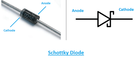
Schottky diodes, commonly known as barrier diodes or hot-carrier diodes, are metal semiconductors with distinctively low voltage drops and possess a fast switching action. These are formed by the junction of a semiconductor with a metal. The N-type material in these diodes is linked with a metal-semiconductor thereby making the forward voltage drop almost 70% lower in comparison to the PN junction diodes. Metals like Platinum or Aluminum are used instead of the P-type semiconductor. The forward voltage produced ranges on an average between 150mV to 300mV at the maximum.
Read Also:
Basic Working Principle
[Click Here for Sample Questions]
The fundamental principle of operation is based on the Schottky Diode Theory. The low voltage drop and the quick switching rate play important roles in its working. The N-type semiconductor has greater potential energy than that of electrons of metals. As a result, there is a deficiency of a depletion layer at the diode junction making it impossible to store charges. The current thus flows directly through the diode whenever there is a voltage drop. The metal-semiconductor acts as the anode towards which the free electrons move, and the N-type functions as cathode facilitating easier current flow in comparison to PN junction diodes. The stored voltage at the N-type cathode acts like a barrier restricting the backward movement of electrons towards the metal anode.
The drop in the case of a Schottky diode ranges between 0.15 to 0.45V in comparison to PN junction with a drop of 0.6 to 0.7V. Greater efficiency and better output are some advantages of the low voltage drop in Schottky diodes.
Symbol and Construction of Schottky Diode
[Click Here for Sample Questions]
Schottky Diode has the metal as its anode and the semiconductor as the cathode. The anode section is usually materials like Molybdenum, Chromium, Tungsten, or Platinum. The N-type semiconductor is intrinsically doped with Phosphorus, Arsenic, or is an integration of Silicon and Bismuth. Following is the symbol of a Schottky Diode with its construction. The semiconductor end is a highly conductive end called Silicide which provides a very low Ohmic resistance value and thus increases the current flow.

The metal-semiconductor junction acts as a stable unipolar device. The flow of current makes the electrons go from the semiconductor to the metal anode. The current flow is affected by the depletion in charge carriers at the junction as conduction through the diode is blocked due to the absence of a P-type semiconductor. This restricts current backflow and provides a uni-directional pathway for the current.
Characteristics of Schottky Diode
[Click Here for Sample Questions]
The V-I characteristics of a Schottky Diode in comparison to a PN junction diode can be plotted as follows:
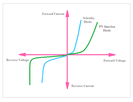
V-I characteristics in a Schottky and PN junction diode
Current is the dependable variable and voltage is the independent variable. The forward voltage drop can be noted to be lower in comparison to the PN junction diode. As the doping concentration is increased, the forward voltage drop also increases. The metal does not allow any charge storage thereby permitting fast switching with a minimal noise component. This diode also functions like a unipolar device due to the lack of electron flow from metal to the N-type semiconductor.
Advantages and Disadvantages of Schottky Diode
[Click Here for Sample Questions]
Let us list down the pros and cons of the Schottky diode.
Advantages
- Shorter recovery time, i.e., time-lapse from switch on to switch off is very small.
- The absence of a depletion layer allows increased current flow.
- Low capacitance owing to the almost negligible depletion layer.
- Operable at high-frequency areas.
- Very low turn-on voltage ranging from 0.15 to 0.3V.
Disadvantages
- High reverse saturation of current flow.
- Prone to leakages at the metal-conductor junction causing heating up of the diode.
Applications of Schottky Diode
[Click Here for Sample Questions]
- Voltage clamping is a common application of Schottky Diodes that prevents transistor saturation owing to the low forward voltage drop.
- Used in Switch Mode Power Supply (SMPS) in laptops, computers, etc because of its fast switching mechanism.
- Used as ‘blocking diodes’ in stand-alone photovoltaic systems. The diodes with their low forward voltage drop, prevent batteries from discharging through the solar panels at night.
- Employed as power dividers in OR circuits due to the high density of current and voltage drops, thereby causing less power wastage in comparison to PN junction diode.
- Used as radiofrequency mixers for high frequency and fast switching speed.
Things to Remember
- Schottky diodes are formed by the junction of an N-type semiconductor (cathode) with a metal (anode).
- Low voltage drop and a fast switching rate are key factors for varied applications of a Schottky diode.
- The voltage drop ranges from 0.15 to 0.45V in comparison to PN junction diodes wherein the voltage drop ranges from 0.6 to 0.1.7V.
- Schottky diodes can be used as unipolar devices due to the absence of a depletion layer at the metal-conductor junction of the diode.
- The reverse saturation of the Schottky diodes is very large making them susceptible to leakages.
- Schottky diodes are used as rectifiers, power dividers, RF mixers, and blocking diodes in photovoltaic applications.
Read More:
Sample Questions
Ques: Explain the significance of Schottky diodes. (2 marks)
Ans: The following characteristic properties of Schottky diodes make them usable for a wide variety of applications:
- Low turn-on voltage
- Fast recovery time
- Low energy loss at higher frequency areas
These properties of the Schottky diode help in rectifying current by quickly switching from turn-on to shut-off mode.
Ques: Differentiate between Schottky and PN junction diodes. (5 marks)
Ans: The difference between Schottky and PN junction diodes are:
| Schottky Diode | PN Junction Diode |
|---|---|
| Formed from the junction between metal and N-type semiconductor | Formed by the junction between P and N-type semiconductors. |
| The flow of current is due to the flow of electrons only. | The flow of current is due to electrons and holes. |
| Functions as a unipolar device. | Functions as a bipolar device. |
| Reverse saturation is lower than normal diodes. | Reverse saturation is greater than Schottky diode. |
| The depletion layer is absent. | The depletion layer is present. |
| The turn-on voltage is less than the normal diodes. | Turn-on voltage is high. |
| Electrons are the majority charge carriers in metallic and semiconductor regions. | Electrons are majority charge carriers in the N region and minority charge carriers in the P region. |
| Temperature dependency is almost nil. | Temperature dependency is needed. |
Ques: What is meant by high reverse saturation? (3 marks)
Ans: High reverse saturation is a major drawback of the Schottky diodes. This affects the diode functioning. The major causes of failure are from wear-out mechanisms particularly in cases where they are used at the output of power supplies. The single reverse current effect is so large at this point that an electric overstress is created thereby rapidly increasing the temperature of the diode. An assembly failure due to these alterations in operating characteristics is mostly the cause of a direct diode failure.
Ques: Which metal is used in the Schottky diode? How is it different from conventional diodes? (3 marks)
Ans: The Schottky diode is formed by the junction of metal with an N-type of semiconductor material. One side of the junction is hence, metal and the other side is silicon dopped. Silicide is the most commonly used metal component owing to the highly conducive Silicon used. This provides the diode with a low Ohm resistance value allowing more current to pass through the small voltage drop.
Ques: What are the applications of Schottky diode? (4 marks)
Ans: The applications of Schottky diode are as follows:
- Voltage clamping is a common application of Schottky Diodes that prevents transistor saturation owing to the low forward voltage drop.
- Used in Switch Mode Power Supply (SMPS) in laptops, computers, etc because of its fast switching mechanism.
- Used as ‘blocking diodes’ in stand-alone photovoltaic systems. The diodes with their low forward voltage drop, prevent batteries from discharging through the solar panels at night.
- Employed as power dividers in OR circuits due to the high density of current and voltage drops, thereby causing less power wastage in comparison to PN junction diode.
Ques: Discuss the advantages and disadvantages of Schottky diode. (4 marks)
Ans: The advantages of schottky diode are:
- Shorter recovery time, i.e., time-lapse from switch on to switch off is very small.
- The absence of a depletion layer allows increased current flow.
- Low capacitance owing to the almost negligible depletion layer.
- Operable at high-frequency areas.
- Very low turn-on voltage ranging from 0.15 to 0.3V.
The disadvantages of schottky diode are:
- High reverse saturation of current flow.
- Prone to leakages at the metal-conductor junction causing heating up of the diode.
For Latest Updates on Upcoming Board Exams, Click Here: https://t.me/class_10_12_board_updates
Do Check Out:



Comments